Mitsubishi microcomputers
M16C / 62 Group
SINGLE-CHIP 16-BIT CMOS MICROCOMPUTER
CPU Rewrite Mode (Flash Memory Version)
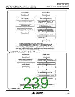
Outline Performance (CPU Rewrite Mode)
In the CPU rewrite mode, the CPU erases, programs and reads the internal flash memory as instructed by
software commands. Operations must be executed from a memory other than the internal flash memory,
such as the internal RAM.
When the CPU rewrite mode select bit (bit 1 at address 03B716) is set to “1”, transition to CPU rewrite mode
occurs and software commands can be accepted.
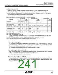
In the CPU rewrite mode, write to and read from software commands and data into even-numbered ad-
dress (“0” for byte address A0) in 16-bit units. Always write 8-bit software commands into even-numbered
address. Commands are ignored with odd-numbered addresses.
Use software commands to control program and erase operations. Whether a program or erase operation
has terminated normally or in error can be verified by reading the status register.
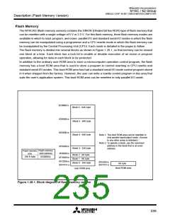
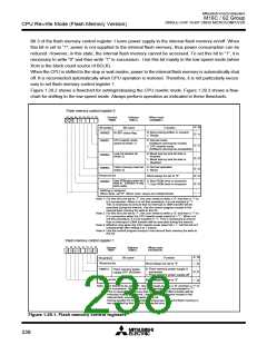
Figure 1.29.1 shows the flash memory control register 0 and the flash memory control register 1.
_____
Bit 0 of the flash memory control register 0 is the RY/BY status flag used exclusively to read the operating
status of the flash memory. During programming and erase operations, it is “0”. Otherwise, it is “1”.
Bit 1 of the flash memory control register 0 is the CPU rewrite mode select bit. The CPU rewrite mode is
entered by setting this bit to “1”, so that software commands become acceptable. In CPU rewrite mode, the
CPU becomes unable to access the internal flash memory directly. Therefore, write bit 1 in an area other
than the internal flash memory. To set this bit to “1”, it is necessary to write “0” and then write “1” in
succession. The bit can be set to “0” by only writing a “0” .
Bit 2 of the flash memory control register 0 is a lock bit disable bit. By setting this bit to “1”, it is possible to
disable erase and write protect (block lock) effectuated by the lock bit data. The lock bit disable select bit
only disables the lock bit function; it does not change the lock data bit value. However, if an erase operation
is performed when this bit =“1”, the lock bit data that is “0” (locked) is set to “1” (unlocked) after erasure. To
set this bit to “1”, it is necessary to write “0” and then write “1” in succession. This bit can be manipulated
only when the CPU rewrite mode select bit = “1”.
Bit 3 of the flash memory control register 0 is the flash memory reset bit used to reset the control circuit of
the internal flash memory. This bit is used when exiting CPU rewrite mode and when flash memory access
has failed. When the CPU rewrite mode select bit is “1”, writing “1” for this bit resets the control circuit. To
release the reset, it is necessary to set this bit to “0”.
Bit 5 of the flash memory control register 0 is a user ROM area select bit which is effective in only boot
mode. If this bit is set to “1” in boot mode, the area to be accessed is switched from the boot ROM area to
the user ROM area. When the CPU rewrite mode needs to be used in boot mode, set this bit to “1”. Note
that if the microcomputer is booted from the user ROM area, it is always the user ROM area that can be
accessed and this bit has no effect. When in boot mode, the function of this bit is effective regardless of
whether the CPU rewrite mode is on or off. Use the control program except in the internal flash memory to
rewrite this bit.
237

 MITSUBISHI [ Mitsubishi Group ]