Mitsubishi microcomputers
M16C / 62 Group
SINGLE-CHIP 16-BIT CMOS MICROCOMPUTER
CPU Rewrite Mode (Flash Memory Version)
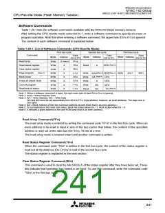
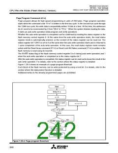
Page Program Command (4116)
Page program allows for high-speed programming in units of 256 bytes. Page program operation
starts when the command code “4116” is written in the first bus cycle. In the second bus cycle through
the 129th bus cycle, the write data is sequentially written 16 bits at a time. At this time, the addresses
A0-A7 need to be incremented by 2 from “0016” to “FE16.” When the system finishes loading the data,
it starts an auto write operation (data program and verify operation).
Whether the auto write operation is completed can be confirmed by reading the status register or the
flash memory control register 0. At the same time the auto write operation starts, the read status
register mode is automatically entered, so the content of the status register can be read out. The
status register bit 7 (SR7) is set to 0 at the same time the auto write operation starts and is returned to
1 upon completion of the auto write operation. In this case, the read status register mode remains
active until the Read Array command (FF16) or Read Lock Bit Status command (7116) is written or the
flash memory is reset using its reset bit.
____
The RY/BY status flag of the flash memory control register 0 is 0 during auto write operation and 1
when the auto write operation is completed as is the status register bit 7.
After the auto write operation is completed, the status register can be read out to know the result of the
auto write operation. For details, refer to the section where the status register is detailed.
Figure 1.29.4 shows an example of a page program flowchart.
Each block of the flash memory can be write protected by using a lock bit. For details, refer to the
section where the data protect function is detailed.
Additional writes to the already programmed pages are prohibited.
Start
Write 4116
n = 0
Write address n and
n = n + 2
data n
NO
n = FE16
YES
NO
RY/BY status flag
= 1?
YES
Check full status
Page program
completed
Figure 1.29.4. Page program flowchart
242

 MITSUBISHI [ Mitsubishi Group ]