Mitsubishi microcomputers
M16C / 61 Group
SINGLE-CHIP 16-BIT CMOS MICROCOMPUTER
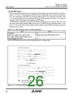
Bus Control
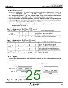
(8) BCLK output
The user can choose the BCLK output by use of bit 7 of processor mode register 0 (000416) (Note).
When set to “1”, the output floating.
Note: Before attempting to change the contents of the processor mode register 0, set bit 1 of the protect
register (address 000A16) to “1”.
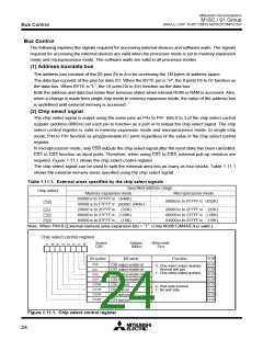
(9) Software wait
A software wait can be inserted by setting the wait bit (bit 7) of the processor mode register 1 (address
000516) (Note) and bits 4 to 7 of the chip select control register (address 000816).
A software wait is inserted in the internal ROM/RAM area and in the external memory area by setting the
wait bit of the processor mode register 1. When set to “0”, each bus cycle is executed in one BCLK cycle.
When set to “1”, each bus cycle is executed in two or three BCLK cycles. After the microcomputer has been
reset, this bit defaults to “0”. When set to “1”, a wait is applied to all memory areas (two or three BCLK
cycles), regardless of the contents of bits 4 to 7 of the chip select control register. Set this bit after referring
to the recommended operating conditions (main clock input oscillation frequency) of the electric character-
________
istics. However, when the user is using the RDY signal, the relevant bit in the chip select control register’s
bits 4 to 7 must be set to “0”.
When the wait bit of the processor mode register 1 is “0”, software waits can be set independently for
each of the 4 areas selected using the chip select signal. Bits 4 to 7 of the chip select control register
_______
_______
correspond to chip selects CS0 to CS3. When one of these bits is set to “1”, the bus cycle is executed in
one BCLK cycle. When set to “0”, the bus cycle is executed in two or three BCLK cycles. These bits
default to “0” after the microcomputer has been reset.
The SFR area is always accessed in two BCLK cycles regardless of the setting of these control bits. Also,
insert a software wait if using the multiplex bus to access the external memory area.
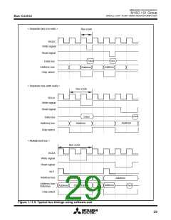
Table 1.11.7 shows the software wait and bus cycles. Figure 1.11.5 shows example bus timing when
using software waits.
Note: Before attempting to change the contents of the processor mode register 1, set bit 1 of the protect
register (address 000A16) to “1”.
Table 1.11.7. Software waits and bus cycles
Bits 4 to 7 of chip select
Bus cycle
2 BCLK cycles
Area
SFR
Bus status
Wait bit
control register
Invalid
0
Invalid
Invalid
1 BCLK cycle
Internal
ROM/RAM
1
0
0
Invalid
2 BCLK cycles
1 BCLK cycle
2 BCLK cycles
Separate bus
Separate bus
Separate bus
1
0
External
memory
area
1
0
1
0 (Note)
0
2 BCLK cycles
3 BCLK cycles
3 BCLK cycles
Multiplex bus
Multiplex bus
0 (Note)
Note: When using the RDY signal, always set to “0”.
28

 MITSUBISHI [ Mitsubishi Group ]