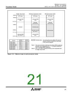
Mitsubishi microcomputers
M16C / 61 Group
SINGLE-CHIP 16-BIT CMOS MICROCOMPUTER
Bus Control
(3) Read/write signals
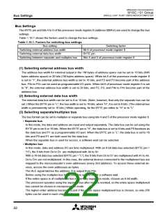
With a 16-bit data bus (BYTE pin =“L”), bit 2 of the processor mode register 0 (address 000416) select the
_____ ________
______
_____ ________
_________
combinations of RD, BHE, and WR signals or RD, WRL, and WRH signals. With an 8-bit data bus (BYTE
_____ ______
_______
pin = “H”), use the combination of RD, WR, and BHE signals. (Set bit 2 of the processor mode register 0
(address 000416) to “0”.) Tables 1.11.2 and 1.11.3 show the operation of these signals.
_____ ______
________
After a reset has been cancelled, the combination of RD, WR, and BHE signals is automatically selected.
_____ _________
_________
When switching to the RD, WRL, and WRH combination, do not write to external memory until bit 2 of the
processor mode register 0 (address 000416) has been set (Note).
Note: Before attempting to change the contents of the processor mode register 0, set bit 1 of the protect
register (address 000A16) to “1”.
_____ ________
_________
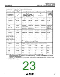
Table 1.11.2. Operation of RD, WRL, and WRH signals
Data bus width
Status of external data bus
RD
L
WRL
H
L
WRH
H
H
L
Read data
H
Write 1 byte of data to even address
Write 1 byte of data to odd address
Write data to both even and odd addresses
16-bit
(BYTE = “L”)
H
H
L
H
L
_____ ______
________
Table 1.11.3. Operation of RD, WR, and BHE signals
Data bus width
A0
H
Status of external data bus
Write 1 byte of data to odd address
Read 1 byte of data from odd address
Write 1 byte of data to even address
Read 1 byte of data from even address
Write data to both even and odd addresses
Read data from both even and odd addresses
Write 1 byte of data
RD
H
L
WR
L
BHE
L
H
L
L
H
16-bit
(BYTE = “L”)
H
L
H
L
H
L
H
L
H
L
L
L
H
L
L
L
H
L
Not used
Not used
H / L
H / L
8-bit
(BYTE = “H”)
H
Read 1 byte of data
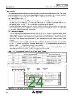
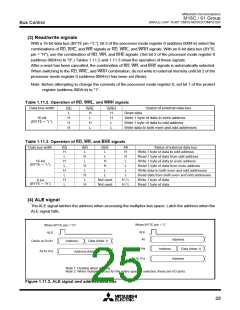
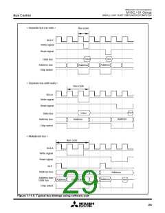
(4) ALE signal
The ALE signal latches the address when accessing the multiplex bus space. Latch the address when the
ALE signal falls.
When BYTE pin = “L”
ALE
When BYTE pin = “H”
ALE
A
0
Address
Data (Note 1)
Address
Data (Note 1)
D0/A0 to D7/A7
D0/A1 to D7/A8
Address
A8 to A19
Address (Note 2)
A9 to A19
Address
Note 1: Floating when reading.
Note 2: When multiplexed bus for the entire space is selected, these are I/O ports.
Figure 1.11.2. ALE signal and address/data bus
25

 MITSUBISHI [ Mitsubishi Group ]