Mitsubishi microcomputers
M16C / 61 Group
SINGLE-CHIP 16-BIT CMOS MICROCOMPUTER
Bus Control
Bus Control
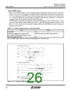
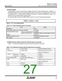
The following explains the signals required for accessing external devices and software waits. The signals
required for accessing the external devices are valid when the processor mode is set to memory expansion
mode and microprocessor mode. The software waits are valid in all processor modes.
(1) Address bus/data bus
The address bus consists of the 20 pins A0 to A19 for accessing the 1M bytes of address space.
The data bus consists of the pins for data I/O. When the BYTE pin is “H”, the 8 ports D0 to D7 function as
the data bus. When BYTE is “L”, the 16 ports D0 to D15 function as the data bus.
Both the address and data bus retain their previous states when internal ROM or RAM is accessed. Also,
when a change is made from single-chip mode to memory expansion mode, the value of the address bus
is undefined until external memory is accessed.
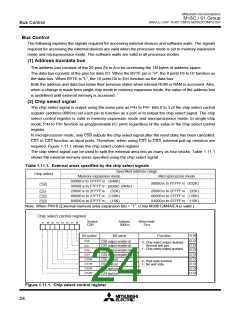
(2) Chip select signal
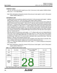
The chip select signal is output using the same pins as P44 to P47. Bits 0 to 3 of the chip select control
register (address 000816) set each pin to function as a port or to output the chip select signal. The chip
select control register is valid in memory expansion mode and microprocessor mode. In single-chip
mode, P44 to P47 function as programmable I/O ports regardless of the value in the chip select control
register.
_______
In microprocessor mode, only CS0 outputs the chip select signal after the reset state has been cancelled.
_______
_______
_______
_______
CS1 to CS3 function as input ports. Therefore, when using CS1 to CS3, external pull-up resistors are
required. Figure 1.11.1 shows the chip select control register.
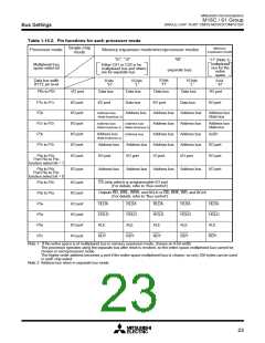
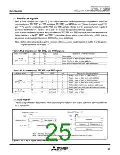
The chip select signal can be used to split the external area into as many as four blocks. Table 1.11.1
shows the external memory areas specified using the chip select signal.
Table 1.11.1. External areas specified by the chip select signals
Specified address range
Chip select
Memory expansion mode
Microprocessor mode
3000016 to CFFFF16 (640K)
3000016 to FFFFF16 (832K)
CS0
3000016 to F7FFF16
2800016 to 2FFFF16
(Note)
(800K)
(32K)
2800016 to 2FFFF16 (32K)
0800016 to 27FFF16 (128K)
0400016 to 07FFF16 (16K)
CS1
CS2
CS3
0800016 to 27FFF16 (128K)
0400016 to 07FFF16 (16K)
Note: When PM16 (External memory area expansion bit) = “1”. (Only M30612M4A/E4 is valid.)
Chip select control register
Symbol
CSR
Address
000816
When reset
0116
b7 b6 b5 b4 b3 b2 b1 b0
R W
Bit symbol
Bit name
Function
CS0
CS0 output enable bit
CS1 output enable bit
CS2 output enable bit
CS3 output enable bit
0 : Chip select output disabled
(Normal port pin)
1 : Chip select output enabled
CS1
CS2
CS3
CS0W
CS1W
CS2W
CS3W
CS0 wait bit
CS1 wait bit
CS2 wait bit
CS3 wait bit
0 : Wait state inserted
1 : No wait state
Figure 1.11.1. Chip select control register
24

 MITSUBISHI [ Mitsubishi Group ]