Mitsubishi microcomputers
M16C / 61 Group
SINGLE-CHIP 16-BIT CMOS MICROCOMPUTER
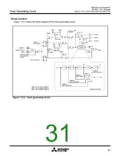
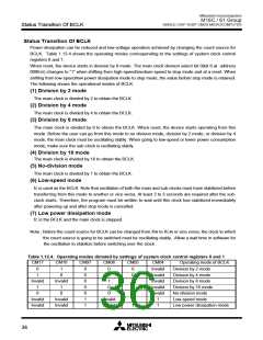
Clock Generating Circuit
The following paragraphs describes the clocks generated by the clock generating circuit.
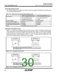
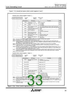
(1) Main clock
The main clock is generated by the main clock oscillation circuit. After a reset, the clock is divided by 8 to
the BCLK. The clock can be stopped using the main clock stop bit (bit 5 at address 000616). Stopping the
clock, after switching the operating clock source of CPU to the sub-clock, reduces the power dissipation.
After the oscillation of the main clock oscillation circuit has stabilized, the drive capacity of the main clock
oscillation circuit can be reduced using the XIN-XOUT drive capacity select bit (bit 5 at address 000716).
Reducing the drive capacity of the main clock oscillation circuit reduces the power dissipation. This bit
changes to “1” when shifting from high-speed/medium-speed mode to stop mode and at a reset. When
shifting from low-speed/low power dissipation mode to stop mode, the value before stop mode is re-
tained.
(2) Sub-clock
The sub-clock is generated by the sub-clock oscillation circuit. No sub-clock is generated after a reset.
After oscillation is started using the port Xc select bit (bit 4 at address 000616), the sub-clock can be
selected as the BCLK by using the system clock select bit (bit 7 at address 000616). However, be sure
that the sub-clock oscillation has fully stabilized before switching.
After the oscillation of the sub-clock oscillation circuit has stabilized, the drive capacity of the sub-clock
oscillation circuit can be reduced using the XCIN-XCOUT drive capacity select bit (bit 3 at address 000616).
Reducing the drive capacity of the sub-clock oscillation circuit reduces the power dissipation. This bit
changes to “1” when shifting to stop mode and at a reset.
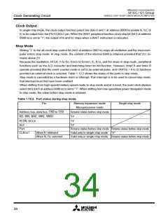
(3) BCLK
The BCLK is the clock that drives the CPU, and is fc or the clock is derived by dividing the main clock by
1, 2, 4, 8, or 16. The BCLK is derived by dividing the main clock by 8 after a reset. The BCLK signal can
be output from BCLK pin by the BCLK output disable bit (bit 7 at address 000416) in the memory expan-
sion and the microprocessor modes.
The main clock division select bit 0(bit 6 at address 000616) changes to “1” when shifting from high-
speed/medium-speed to stop mode and at reset. When shifting from low-speed/low power dissipation
mode to stop mode, the value before stop mode is retained.
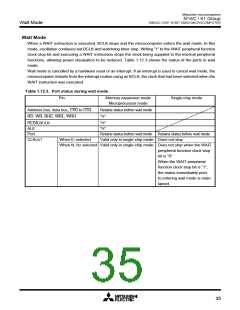
(4) Peripheral function clock(f1, f8, f32, f1SIO2, f8SIO2,f32SIO2,fAD)
The clock for the peripheral devices is derived from the main clock or by dividing it by 1, 8, or 32. The
peripheral function clock is stopped by stopping the main clock or by setting the WAIT peripheral function
clock stop bit (bit 2 at 000616) to “1” and then executing a WAIT instruction.
(5) fC32
This clock is derived by dividing the sub-clock by 32. It is used for the timer A and timer B counts.
(6) fC
This clock has the same frequency as the sub-clock. It is used for the BCLK and for the watchdog timer.
32

 MITSUBISHI [ Mitsubishi Group ]