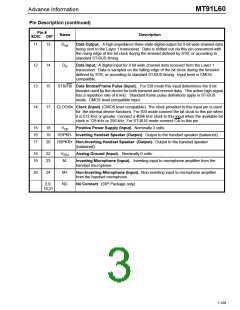
Advance Information
MT91L60
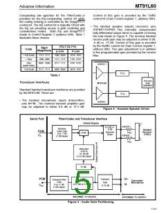
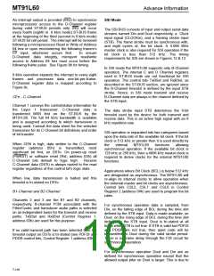
The data streams operate at 2048 kb/s and are Time
Division Multiplexed into 32 identical channels of 64
kb/s bandwidth. A frame pulse (a 244 nSec low going
pulse) is used to parse the continuous serial data
streams into the 32 channel TDM frames. Each
frame has a 125 µSecond period translating into an 8
kHz frame rate. A valid frame begins when F0i is
logic low coincident with a falling edge of C4i. Refer
to Figure 11 for detailed ST-BUS timing. C4i has a
frequency (4096 kHz) which is twice the data rate.
This clock is used to sample the data at the 3/4
bit-cell position on DSTi and to make data available
on DSTo at the start of the bit-cell. C4i is also used to
clock the MT91L60 internal functions (i.e., Filter/
➃
➄
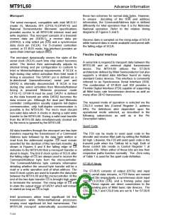
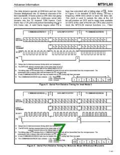
COMMAND/ADDRESS
DATA INPUT/OUTPUT
COMMAND/ADDRESS:
➀
➀
DATA 1
RECEIVE
D0 D1 D2 D3 D4 D5 D6 D7
D0 D1 D2 D3 D4 D5 D6 D7
D0 D1 D2 D3 D4 D5 D6 D7
D0 D1 D2 D3 D4 D5 D6 D7
D0 D1 D2 D3 D4 D5 D6 D7
DATA 1
TRANSMIT
②
SCLK
CS
➃
➂
➂
➀
②
Delays due to internal processor timing which are transparent.
The MT91L60:-latches received data on the rising edge of SCLK.
-outputs transmit data on the falling edge of SCLK.
➂
The falling edge of CS indicates that a COMMAND/ADDRESS byte will be transmitted from the microprocessor. The
subsequent byte is always data until terminated via CS returning high.
➃
➄
A new COMMAND/ADDRESS byte may be loaded only by CS cycling high then low again.
D7
D0
The COMMAND/ADDRESS byte contains: 1 bit - Read/Write
3 bits - Addressing Data
X
X
X
X
A2
A1
A0
R/W
4 bits - Unused
Figure 5 - Serial Port Relative Timing for Intel Mode 0
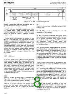
➃
COMMAND/ADDRESS
DATA INPUT/OUTPUT
COMMAND/ADDRESS:
➄
➀
➀
DATA 2
RECEIVE
D7 D6 D5 D4 D3 D2 D1 D0
D7 D6 D5 D4 D3 D2 D1 D0
D7 D6 D5 D4 D3 D2 D1 D0
D7 D6 D5 D4 D3 D2 D1 D0
D7 D6 D5 D4 D3 D2 D1 D0
DATA 1
TRANSMIT
②
SCLK
CS
➃
➂
➂
➀
②
Delays due to internal processor timing which are transparent .
The MT91L60:-latches received data on the rising edge of SCLK.
-outputs transmit data on the falling edge of SCLK.
➂
The falling edge of CS indicates that a COMMAND/ADDRESS byte will be transmitted from the microprocessor. The
subsequent byte is always data until terminated via CS returning high.
➃
➄
A new COMMAND/ADDRESS byte may be loaded only by CS cycling high then low again.
D7
D0
X
The COMMAND/ADDRESS byte contains: 1 bit - Read/Write
3 bits - Addressing Data
4 bits - Unused
A2
R/W
X
X
X
A1
A0
Figure 6 - Serial Port Relative Timing for Motorola Mode 00/National Microwire
7-113

 MITEL [ MITEL NETWORKS CORPORATION ]