Advance Information
MT91L60
the resynchronization circuitry activity and will not
affect operation since the bit cell period at 128 kb/s
and 256 kb/s is relatively large. There is a one frame
delay through the FDI circuit for asynchronous
operation. Refer to the specifications of Figures 12
& 13 for both synchronous and asynchronous SSI
timing.
After Power-up reset (PWRST) or software reset
(Rst) all control bits assume their default states;
µ-Law functionality, usually 0 dB programmable
gains as well as the device powered up in SSI mode
2048 kb/s operation with Dout tri-stated while there
is no strobe active on STB. If a valid strobe is
supplied to STB, then Dout will be active, during the
defined channel.
PWRST/Software Reset (Rst)
To attain complete power-down from a normal
operating condition, write PDFDI = 1 and PDDR = 1
(Control Register 1, address 03h) or put PWRST pin
low.
While the MT91L60 is held in PWRST no device
control or functionality is possible. While in software
reset (Rst=1, address 03h) only the microport is
functional. Software reset can only be removed by
writing Rst logic low or by setting the PWRST pin.
3V Multi-featured Codec Register Map
00
01
RxINC
-
RxFG
RxFG
RxFG
TxINC
TxFG
TxFG
TxFG
0
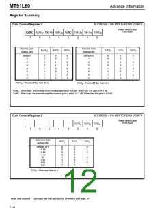
Gain Control
Register 1
2
1
0
2
1
-
-
-
-
STG
-
STG
-
STG
0
Gain Control
Register 2
2
1
02
03
-
-
-
-
-
-
DrGain
R Bsel
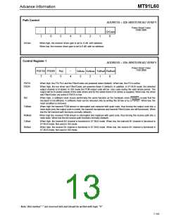
Path Control
PDFDI
PDDR
DEN
RST
T Mute
R Mute
T Bsel
Control
Register 1
x
x
x
x
04
05
06
07
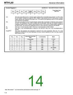
CEN
D8
A/µ
Smag/
ITU-T
CSL
CSL
CSL
0
Control
Register 2
2
1
C
D
-
C
D
-
C
D
-
C
D
-
C
C
D
C
D
-
C
D
-
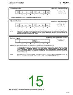
C-Channel
Register
7
7
6
6
5
5
4
4
3
2
2
1
1
0
0
D
D-Channel
Register
3
PCM/
loopen
Loop Back
ANALOG
7-117

 MITEL [ MITEL NETWORKS CORPORATION ]