MT91L60
Advance Information
wide dynamic range from a single 5 volt supply
design. This fully differential architecture is
continued into the Transducer Interface section to
provide full chip realization of these capabilities for
the handset functions.
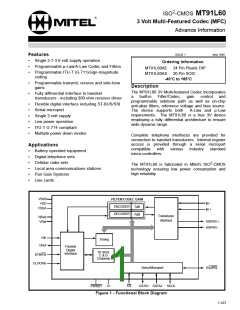
Overview
The 3V Multi-featured Codec (MFC) features
complete
conversion of audio signals (Filter/Codec) and an
analog interface to a standard handset transmitter
and receiver (Transducer Interface). The receiver
amplifier is capable of driving a 300 ohm load.
Analog/Digital
and
Digital/Analog
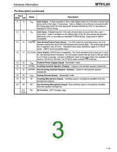
A reference voltage (V ), for the conversion
Ref
requirements of the Codec section, and a bias
voltage (V
), for biasing the internal analog
Bias
sections, are both generated on-chip. V
brought to an external pin so that it may be used for
biasing external gain setting amplifiers. A 0.1µF
is also
Bias
Each of the programmable parameters within the
functional blocks is accessed through a serial
microcontroller port compatible with Intel MCS-51 ,
®
capacitor must be connected from V
to analog
may only
®
Bias
Motorola SPI
and National Semiconductor
ground at all times. Likewise, although V
®
Ref
Microwire specifications. These parameters include:
gain control, power down, mute, B-Channel select
(ST-BUS mode), C&D channel control/access, law
control, digital interface programming and loopback.
Optionally the device may be used in a controllerless
mode utilizing the power-on default settings.
be used internally, a 0.1µF capacitor from the V
Ref
pin to ground is required at all times. The analog
ground reference point for these two capacitors must
be physically the same point. To facilitate this the
V
and V
pins are situated on adjacent pins.
Ref
Bias
The transmit filter is designed to meet ITU-T G.714
specifications. The nominal gain for this filter is 0 dB
(gain control = 0 dB). Gain control allows the output
signal to be increased up to 7 dB. An anti-aliasing
filter is included. This is a second order lowpass
implementation with a corner frequency at 25 kHz.
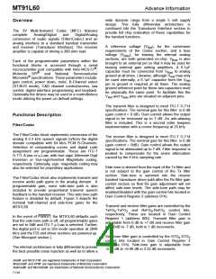
Functional Description
Filter/Codec
The Filter/Codec block implements conversion of the
analog 0-3.3 kHz speech signals to/from the digital
domain compatible with 64 kb/s PCM B-Channels.
Selection of companding curves and digital code
assignment are programmable. These are ITU-T
G.711 A-law or µ-Law, with true-sign/ Alternate Digit
Inversion or true-sign/Inverted Magnitude coding,
respectively. Optionally, sign- magnitude coding may
also be selected for proprietary applications.
The receive filter is designed to meet ITU-T G.714
specifications. The nominal gain for this filter is 0 dB
(gain control = 0dB). Gain control allows the output
signal to be attenuated up to 7 dB. Filter response is
peaked to compensate for the sinx/x attenuation
caused by the 8 kHz sampling rate.
Side-tone is derived from the input of the Tx filter and
is not subject to the gain control of the Tx filter
section. Side-tone is summed into the receive
handset transducer driver path after the Rx filter gain
control section so that Rx gain adjustment will not
affect side-tone levels. The side-tone path may be
enabled/disabled with the gain control bits located in
Gain Control Register 2 (address 01h).
The Filter/Codec block also implements transmit and
receive audio path gains in the analog domain. A
programmable gain, voice side-tone path is also
included to provide proportional transmit speech
feedback to the handset receiver. This side tone path
feature is disabled by default. Figure 3 depicts the
nominal half-channel and side-tone gains for the
MT91L60.
Transmit and receive filter gains are controlled by the
TxFG -TxFG
and RxFG -RxFG
control bits,
0
2
0
2
respectively. These are located in Gain Control
Register 1 (address 00h). Transmit filter gain is
adjustable from 0 dB to +7 dB and receive filter gain
from 0dB to -7 dB, both in 1 dB increments.
In the event of PWRST, the MT91L60 defaults such
that the side-tone path is off, all programmable gains
are set to 0dB and ITU-T µ-Law is selected. Further,
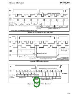
the digital port is set to SSI mode operation at 2048
kb/s and the FDI and driver sections are powered up.
(See Microport section.)
Side-tone filter gain is controlled by the STG -STG
0
2
control bits located in Gain Control Register 2
(address 01h). Side-tone gain is adjustable from
-9.96 dB to +9.96 dB in 3.32 dB increments.
The internal architecture is fully differential to provide
the best possible noise rejection as well as to allow a
Intel® and MCS-51® are registered trademarks of Intel Corporation
Motorola® and SPI® are registered trademarks of Motorola Corporation
National® and Microwire® are trademarks of National Semiconductor Corporation
7-110

 MITEL [ MITEL NETWORKS CORPORATION ]