MT9092
To facilitate this the V
on adjacent pins.
and V
pins are situated
Bias
Both of these reside in the General Control Register
(address 0Fh).
Ref
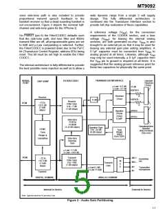
The transmit filter is designed to meet CCITT G.714
specifications. The nominal gain for this filter path is
0dB (gain control = 0dB). An anti-aliasing filter is
Digital Signal Processor
The DSP block is located, functionally, between the
serial ST-BUS port and the Filter/CODEC block. Its
main purpose is to provide both a digital gain control
and a half-duplex handsfree switching function. The
DSP will also generate the digital patterns required
to produce standard DTMF signalling tones as well
as single tones and a tone ringer output. A
programmable (ON/OFF) offset null routine may also
be performed on the transmit PCM data stream. The
DSP can generate a ringer tone to be applied to the
speakerphone speaker during normal handset
operation so that the existing call is not interrupted.
included. This is
a
second order lowpass
implementation with a corner frequency at 25kHz.
Attenuation is better than 32dB at 256 kHz and less
than 0.01dB within the passband.
An optional 400Hz high-pass function may be
included into the transmit path by enabling the Tfhp
bit in the Transducer Control Register (address 0Eh).
This option allows the reduction of transmitted
background noise such as motor and fan noise.
The receive filter is designed to meet CCITT G.714
specifications. The nominal gain for this filter path is
0 dB (gain control = 0dB). Filter response is peaked
to compensate for the sinx/x attenuation caused by
the 8kHz sampling rate.
The main functional control of the DSP is through
two hardware registers which are accessible at any
time via the microport. These are the Receive Gain
Control Register at address 1Dh and the DSP
Control Register at address 1Eh. In addition, other
functional control is accomplished via multiple RAM-
based registers which are accessible only while the
DSP is held in a reset state. This is accomplished
with the DRESET bit of the DSP Control Register.
Ram-based registers are used to store transmit gain
levels (20h for transmit PCM and 21h for transmit
DTMF levels), the coefficients for tone and ringer
generation (addresses 23h and 24h), and tone ringer
warble rates (address 26h). All undefined addresses
below 20h are reserved for the temporary storage of
interim variables calculated during the execution of
the DSP algorithms. These undefined addresses
should not be written to via the microprocessor port.
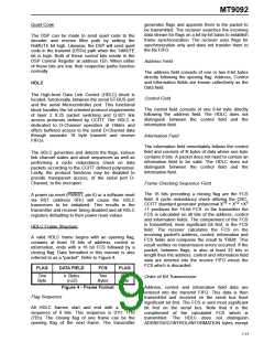
The DSP can be programmed to execute the
following micro-programs which are stored in
instruction ROM, (see PS0 to PS2, DSP Control
Register, address 1Eh). All program execution
begins at the frame pulse boundary.
The Rx filter function can be altered by enabling the
DIAL EN control bit in the Transducer Control
Register (address 0Eh). This causes another
lowpass function to be added, with a 3dB point at
1000Hz. This function is intended to improve the
sound quality of digitally generated dial tone
received as PCM.
Transmit sidetone is derived from the Tx filter and is
subject to the gain control of the Tx filter section.
Sidetone is summed into the receive path after the
Rx filter gain control section so that Rx gain
adjustment will not affect sidetone levels. The side-
tone path may be enabled/disabled with the SIDE
EN bit located in the Transducer Control Register
(address 0Eh). See also STG -STG (address 0Bh).
0
2
Transmit and receive filter gains are controlled by the
TxFG -TxFG and RxFG -RxFG control bits
respectively. These are located in the FCODEC Gain
Control Register 1 (address 0Ah). Transmit filter gain
is adjustable from 0dB to +7dB and receive filter gain
from 0dB to -7dB, both in 1dB increments.
0
2
0
2
PS2
0
PS1 PS0
Micro-program
0
0
0
1
Power up reset program
0
Transmit and receive gain control
program; with autonulling of the
transmit PCM, if the AUTO bit is
set (see address 1Dh)
Side-tone filter gain is controlled by the STG -STG
0
2
0
0
1
1
0
1
DTMF generation plus transmit
control bits located in the FCODEC Gain Control
Register (address 0Bh). Side-tone gain is
and
receive
gain
control
2
program (autonull available via
the AUTO control bit)
adjustable from -9.96dB to +9.96dB in 3.32dB
increments.
Tone ringer plus transmit and
receive gain control program
(autonull available via the
AUTO control bit)
Law selection for the Filter/CODEC is provided by
the A/µ companding control bit while the coding
scheme is controlled by the sign-mag/CCITT bit.
7-8

 MITEL [ MITEL NETWORKS CORPORATION ]