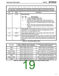
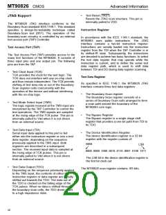
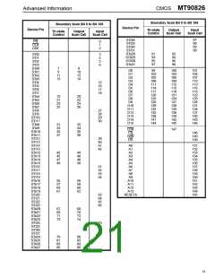
MT90826 CMOS
Advanced Information
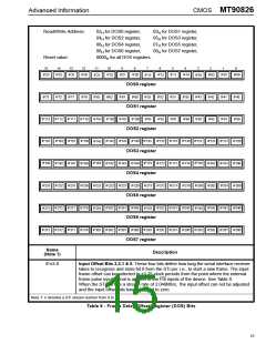
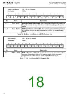
Read/Write Address:
Reset value:
0011 for BISR register,
H
0000
H
15
0
14
0
13
0
12
11
10
BSA2
9
8
7
6
5
4
3
2
1
0
BSA4 BSA3
BSA1 BSA0 BCA7
BCA6 BCA5 BCA4 BCA3 BCA2 BCA1 BCA0
Bit
Name
Description
12 - 8
BSA4 - BSA0
BER Input Stream Address Bits. The number expressed in binary notation on
these bits refers to the input data stream which receives the pseudo random
pattern.
7 - 0
BCA7 - BCA0
BER Input Channel Address Bits. The number expressed in binary notation
on these bits refers to the input channel which receives the pseudo random
pattern.
Table 12 - Bit Error Input Selection (BISR) Register Bits
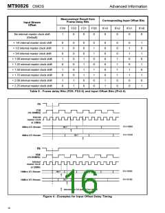
Read Address:
Reset value:
0012 for BECR register,
H
0000
H
15
14
13
12
11
10
9
8
7
6
5
4
3
2
1
0
BER15 BER14 BER13 BER12 BER11 BER10 BER9 BER8 BER7
BER6 BER5 BER4 WR3
WR2
WR1
WR0
Bit
15 - 0
Name
Description
BER15 - BER0
Bit Error Rate Count Bits. The number expressed in binary notation on these
bits refers to the bit error counts. The register content can be cleared by
programming the CBER bit in the control register from zero to one.
Table 13 - Bit Error Count (BECR) Register Bits
18

 MITEL [ MITEL NETWORKS CORPORATION ]