Advanced Information
CMOS MT90826
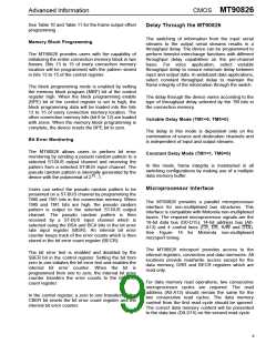
CLK
(CPLL=0)
CLK
(CPLL=1)
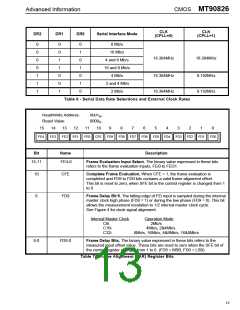
DR2
DR1
DR0
Serial Interface Mode
0
0
0
0
1
1
1
0
0
1
1
0
0
1
0
1
0
1
0
1
0
8 Mb/s
16 Mb/s
16.384MHz
16.384MHz
4 and 8 Mb/s
16 and 8 Mb/s
4 Mb/s
16.384MHz
16.384MHz
8.192MHz
8.192MHz
2 and 4 Mb/s
2 Mb/s
Table 6 - Serial Data Rate Selections and External Clock Rates
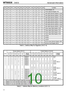
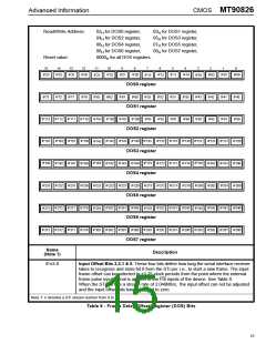
Read/Write Address:
Reset Value:
0001 ,
H
0000 .
H
15
14
13
12
11
10
9
8
7
6
5
4
3
2
1
0
FE4
FE3
FE2 FE1
FE0
CFE
FD9
FD8
FD7
FD6
FD5
FD4
FD3
FD2
FD1
FD0
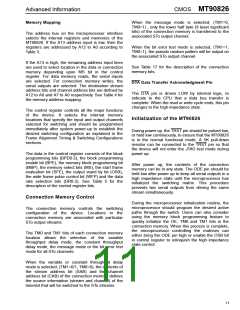
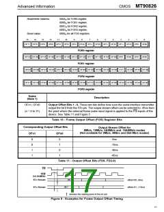
Bit
Name
Description
15-11
10
FE4-0
Frame Evaluation Input Select. The binary value expressed in these bits
refers to the frame evaluation inputs, FEi0 to FEi31.
CFE
FD9
Complete Frame Evaluation. When CFE = 1, the frame evaluation is
completed and FD9 to FD0 bits contains a valid frame alignment offset.
This bit is reset to zero, when SFE bit in the control register is changed from 1
to 0.
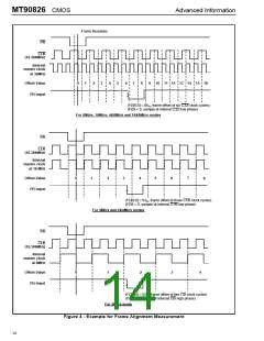
9
Frame Delay Bit 9. The falling edge of FEi input is sampled during the internal
master clock high phase (FD9 = 1) or during the low phase (FD9 = 0). This bit
allows the measurement resolution to 1/2 internal master clock cycle.
See Figure 4 for clock signal alignment.
Internal Master Clock
Operation Mode
2Mb/s
C8i
C16i
C32i
4Mb/s, 2&4Mb/s
8Mb/s, 16Mb/s, 4&8Mb/s, 16&8Mb/s
8-0
FD8-0
Frame Delay Bits. The binary value expressed in these bits refers to the
measured input offset value. These bits are reset to zero when the SFE bit of
the control register changes from 1 to 0. (FD8 = MSB, FD0 = LSB)
Table 7 - Frame Alignment (FAR) Register Bits
13

 MITEL [ MITEL NETWORKS CORPORATION ]