Advanced Information
CMOS MT90826
See Table 10 and Table 11 for the frame output offset
programming.
Delay Through the MT90826
The switching of information from the input serial
streams to the output serial streams results in a
throughput delay. The device can be programmed to
perform timeslot interchange functions with different
throughput delay capabilities on the per-channel
basis. For voice application, select variable
throughput delay to ensure minimum delay between
input and output data. In wideband data applications,
select constant throughput delay to maintain the
frame integrity of the information through the switch.
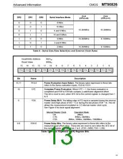
Memory Block Programming
The MT90826 provides users with the capability of
initializing the entire connection memory block in two
frames. Bits 13 to 15 of every connection memory
location will be programmed with the pattern stored
in bits 13 to 15 of the control register.
The block programming mode is enabled by setting
the memory block program (MBP) bit of the control
register high. When the block programming enable
(BPE) bit of the control register is set to high, the
block programming data will be loaded into the bits
13 to 15 of every connection memory location. The
other connection memory bits (bit 0 to 12) are loaded
with zeros. When the memory block programming is
complete, the device resets the BPE bit to zero.
The delay through the device varies according to the
type of throughput delay selected by the TM bits in
the connection memory.
Variable Delay Mode (TM1=0, TM0=0)
The delay in this mode is dependent only on the
combination of source and destination channels and
is independent of input and output streams.
Bit Error Monitoring
The MT90826 allows users to perform bit error
monitoring by sending a pseudo random pattern to a
selected ST-BUS output channel and receiving the
pattern from a selected ST-BUS input channel. The
pseudo random pattern is internally generated by the
Constant Delay Mode (TM1=1, TM0=0)
In this mode, frame integrity is maintained in all
switching configurations by making use of a multiple
data memory buffer.
15
device with the polynomial of 2 -1.
Microprocessor Interface
Users can select the pseudo random pattern to be
presented on a ST-BUS channel by programming the
TM0 and TM1 bits in the connection memory. When
TM0 and TM1 bits are high, the pseudo random
pattern is output to the selected ST-BUS output
channel. The pseudo random pattern is then
received by a ST-BUS input channel which is
selected using the BSA and BCA bits in the bit error
rate input register (BISR). An internal bit error
counter keeps track of the error counts which is then
stored in the bit error count register (BECR).
The MT90826 provides a parallel microprocessor
interface for non-multiplexed bus structures. This
interface is compatible with Motorola non-multiplexed
buses. The required microprocessor signals are the
16-bit data bus (D0-D15), 14-bit address bus (A0-
A13) and 4 control lines (CS, DS, R/W and DTA).
See Figure 14 for Motorola non-multiplexed
microport timing.
The MT90826 microport provides access to the
internal registers, connection and data memories. All
locations provide read/write access except for the
data memory, DRR and BECR registers which are
read only.
The bit error test is enabled and disabled by the
SBER bit in the control register. Setting the bit from
zero to one initiates the bit error test and enables the
internal bit error counter. When the bit is
programmed from one to zero, the internal bit error
counter transfers the error counts to the bit error
count register.
For data memory read operations, two consecutive
microprocessor cycles are required. The read
address (A0-A13) should remain the same for the
two consecutive read cycles. The data memory
content from the first read cycle should be ignored.
The correct data memory content will be presented
to the data bus (D0-D15) on the second read cycle.
In the control register, a zero to one transition of the
CBER bit resets the bit error count register and the
internal bit error counter.
9

 MITEL [ MITEL NETWORKS CORPORATION ]