MT90826 CMOS
Advanced Information
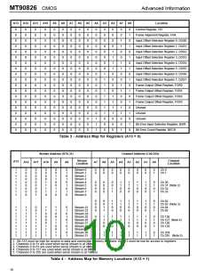
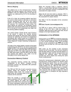
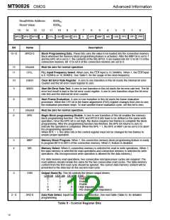
Read/Write Address:
Reset Value:
0000 ,
H
0000 .
H
15
14
13
12
11
10
9
8
7
6
5
4
3
2
1
0
DR2
DR1
DR0
BPD2 BPD1 BPD0
CPLL CBER SBER SFE
0
BPE MBP
MS
OSB
0
Bit
Name
Description
15-13
BPD2-0
Block Programming Data. These bits carry the value to be loaded into the connection memory
block whenever the memory block programming feature is activated. After the MBP bit is set to 1
and the BPE bit is set to 1, the contents of the bits BPD2- 0 are loaded into bit 15 to bit 13 of the
connection memory. Bit 12 to bit 0 of the connection memory are set to 0.
12
11
Unused
CPLL
Must be zero for normal operation.
PLL Input Frequency Select. When zero, the CLK input is 16.384MHz. When 1, the CLK input
is 8.192MHz or 16.384MHz. See Table 6 for the usage of the clock frequency.
10
9
CBER
SBER
Clear Bit Error Rate Register. A zero to one transition in this bit resets the internal bit error
counter and the bit error count register to zero.
Start Bit Error Rate Test. A zero to one transition in this bit starts the bit error rate test. The bit
error test result is kept in the bit error count register. A one to zero transition stops the bit error
rate test and the internal bit error counter.
8
SFE
Start Frame Evaluation. A zero to one transition in this bit starts the frame evaluation
procedure. When the CFE bit in the frame alignement (FAR) register changes from zero to one,
the evaluation procedure stops. To start another frame evaluation cycle, set this bit to zero.
7
6
Unused
BPE
Must be zero for normal operation.
Begin Block programming Enable. A zero to one transition of this bit enables the memory
block programming function. The BPE and BPD2-0 bits have to be defined in the same write
operation. Once the BPE bit is set high, the device requires two frames to complete the block
programming. After the programming function has finished, the BPE bit returns to zero to
indicate the operation is completed. When the BPE = 1, the BPE or MBP can be set to 0 to abort
the programming operation.
When BPE = 1, the other bits in the control register must not be changed for two frames to
ensure proper operation.
5
4
MBP
MS
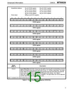
Memory Block Program. When 1, the connection memory block programming feature is ready
to program Bit13 to Bit15 of the connection memory. When 0, feature is disabled.
Memory Select. When 0, connection memory is selected for read or write operations. When 1,
the data memory is selected for read operations and connection memory is selected for write
operations. (No microprocessor write operation is allowed for the data memory.)
For data memory read operations, two consecutive microprocessor cycles are required. The
read address should remain the same for the two consecutive read cycles. The data memory
content from the first read cycle should be ignored. The correct data memory content will be
presented to the data bus on the second read cycle.
3
OSB
Output Stand By. This bit controls the device output drivers.
OSB bit ODE pin OE bit STo0 - 31
0
1
1
0
X
1
0
1
0
X
1
1
1
X
0
Enable
Enable
Enable
High impedance state
Per-channel high impedance
2 - 0
DR2-0
Data Rate Select. Input/Output data rate selection. See next table (Table 6) for detailed
programming.
Table 5 - Control Register Bits
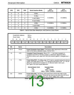
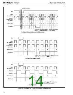
12

 MITEL [ MITEL NETWORKS CORPORATION ]