MT8950 ISO-CMOS
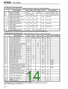
DC Electrical Characteristics
VDD=5.0V±10%; VSS=0V; TA=0oC to 70oC - Voltages are with respect to ground (VSS) unless otherwise stated.
‡
Characteristics
Output LOW voltage
Output HIGH Voltage
Sym
Min
Typ
Max
Units
V
Test Conditions
| I |< 1.0 µA V = 5V
1
2
3
V
0.05
OL
OH
OL
O
DD
V
4.95
2.2
V
| I |< 1.0 µA V = 5V
O
DD
Output LOW Current (On all
outputs except DSTo)
I
2.8
-4.2
11.1
mA
V
V
V
V
=0.4V
OL
O
U
T
P
U
T
4
5
6
7
Output HIGH Current (On all
outputs except DSTo)
I
-3.5
8.9
mA
mA
mA
µA
=2.4V
OH
OH
Output LOW Current (On
DSTo output)
I
=0.4V
OL
OL
S
Output HIGH Current (On
DSTo output)
I
-14.0 -16.8
±1
=2.4V
OH
OH
Output Leakage Current
I
±10
OZ
‡ Typical figures are at 25°C and are for design aid only: not guaranteed and not subject to production testing.
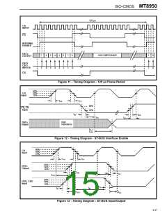
AC Electrical Characteristics† - Voltages are with respect to ground (VSS) unless otherwise stated.
‡
Characteristics
C2i Clock Frequency
C2i Clock Rise Time
C2i Clock Fall Time
Sym
Min
Typ
Max
2.068
50
Units
MHz
ns
Test Conditions
1
2
f
2.028
2.048
CK
t
CR
3
t
50
ns
CF
4
Clock Duty Cycle (C2i & SCLK)
SCLK Clock Frequency
SCLK Clock Rise Time
SCLK Clock Fall Time
F1i and CA Rise Time
F1i and CA Fall Time
F1i and CA Setup Time
F1i and CA Hold Time
DSTo Rise Time
50
%
5
f
0
0.6
128
50
kHz
ns
SCLK
6
t
SCLKR
7
t
50
ns
SCLKF
8
t
100
100
ns
ER
9
t
t
ns
EF
ES
EH
10
11
12
13
14
25
ns
t
-25
25
ns
t
100
100
125
ns
Note 1
Note 1
Note 1
OR
DSTo Fall Time
t
ns
OF
Propagation Delay From Clock
(C2i) To Output (DSTo) enable.
t
ns
PZH
t
PZL
15
Propagation Delay From Clock
(C2i) To Output (DSTo).
t
t
125
ns
Note 1
PLH
PHL
16
17
18
Input Rise Time (DSTi, CSTi)
Input Fall Time (DSTi, CSTi)
t
100
100
ns
ns
ns
IR
t
IF
t
0
ISH
DSTi, CSTi Setup Time
t
ISL
19
20
DSTi, CSTi Hold Time
PRST Low Time
t
90
ns
ns
IH
488
† Timing is over recommended temperature & power supply voltages.
‡ Typical figures are at 25°C and are for design aid only: not guaranteed and not subject to production testing.
Note 1: RL=10KΩ to VDD, CL=150 pF to VSS
6-16

 MITEL [ MITEL NETWORKS CORPORATION ]