ISO-CMOS MT8950
Absolute Maximum Ratings*- Voltages are with respect to ground (VSS) unless otherwise stated.
Parameter
Symbol
Min
Max
Units
1
2
3
4
5
6
7
8
9
Supply Voltage
V
-0.5
7.0
V
DD
DC Input Voltage
DC Output Voltage
V
V
V
-0.3
V
V
+0.3
V
IN
SS
SS
DD
DD
V
-0.3
+0.3
V
OUT
Input Diode Current ( V <0 or V >V
)
I
IK
± 10
± 20
± 25
± 50
150
1.0
mA
mA
mA
mA
I
I
DD
Output Diode Current ( V <0 or V >V
)
I
OK
O
O
DD
DC Output Current, per pin
I
O
DC Supply or Ground Current
StorageTemperature
I
/I
DD SS
o
T
-65
C
ST
o
Package Power Dissipation (CERDIP) T = 25 C
P
W
A
D
* Exceeding these values may cause permanent damage. Functional operation under these conditions is not implied.
Recommended Operating Conditions - Voltages are with respect to ground (VSS) unless otherwise stated.
‡
Characteristics
Supply Voltage
Sym
Min
Typ
Max
Units
Test Conditions
1
2
3
V
4.5
5.0
5.5
V
DD
Operating Frequency
Operating Temperature
f
2.048
MHz
CK
o
T
0
70
C
A
‡ Typical figures are at 25°C and are for design aid only: not guaranteed and not subject to production testing.
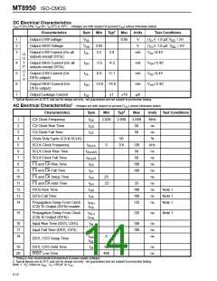
DC Electrical Characteristics
VDD=5.0V±10%; VSS=0V; TA=0oC to 70oC - Voltages are with respect to ground (VSS) unless otherwise stated.
‡
Characteristics
Sym
Min
Typ
Max
Units
Test Conditions
1
2
Quiescent Supply Current
I
150
µA
All outputs unloaded
QS
DD
All inputs @ V
SS
Operating supply current
I
1.0
mA
All outputs unloaded.
Input pins 2 and 3 clocked
at 2.048 MHz.
S
U
P
Pins 1,8,15,20,21 @ V
SS
Pins 5,6,7,9,10,13 and 22
@V
DD
1
3
4
5
TTL inputs
HIGH voltage
LOW voltage
V
V
2.0
V
0.8
V
V
IH
DD
V
IL
SS
2
CMOS inputs
I
HIGH voltage
LOW voltage
V
V
3.5
V
1.5
V
V
IH
DD
N
P
U
T
S
V
IL
SS
3
CMOS Schmitt inputs
HIGH voltage
LOW voltage
V
V
3.0
V
1.0
V
V
IH
DD
V
IL
SS
6
7
8
SPi Comparator ON Voltage
SPi Comparator OFF Voltage
Input Leakage Current
V
2.25
2.5
±1
2.75
V
V
V
V
V
= 5V
T+
DD
DD
DD
V
2.0
= 5V
= 5V
T-
I
±10
µA
IN
‡ Typical figures are at 25°C and are for design aid only: not guaranteed and not subject to production testing.
1. Include DSTi, CSTi, C2i, F1i and SCLK
2. Include DF
3. Include RxE,DX1, DX2 and PRST
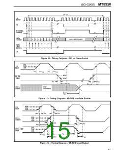
6-15

 MITEL [ MITEL NETWORKS CORPORATION ]