MT8931C
BIT
NAME
DESCRIPTION
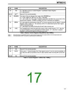
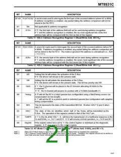
B7-B2 R1A7-R1A2 A six bit mask used to interrogate the first byte of the received address (where B7 is MSB).
If address recognition is enabled, any packet failing the address comparison will not be
stored in the Rx FIFO.
B1
B0
NA
Not applicable to address recognition.
A1En
If ’0’, the first byte of the address field will not be used during address recognition.
If ’1’ and the address recognition is enabled, the six most significant bits of the first
address byte will be compared with the first six bits of this register.
Table 11. HDLC Address Recognition Register 1 (Read/Write Add. 00110B)
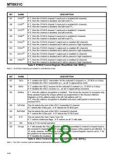
BIT
NAME DESCRIPTION
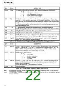
B7-B1 R2A7-R2A1 A seven bit mask used to interrogate the second byte of the received address (where B7
is MSB). If address recognition is enabled, any packet failing the address comparison will
not be stored in the Rx FIFO. This mask is ignored if the address is a Broadcast (i.e., R2A
= 1111111).
B0
A2En
If ’0’, the second byte of the address field will not be used during address recognition.
If ’1’ and the address recognition is enabled, the seven most significant bits of the second
address byte will be compared with the first seven bits of this register.
Table 12. HDLC Address Recognition Register 2 (Read/Write Add. 00111B)
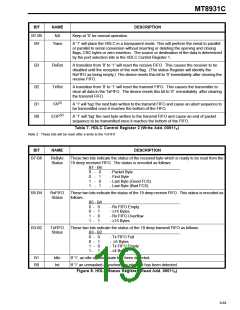
BIT
NAME
DESCRIPTION
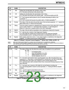
B7
AR
Setting this bit will initiate the activation of the S-Bus.
If ’0’, the device will remain in the present state.
B6
B5
DR
Setting this bit will initiate the deactivation of the S-Bus.
If ’0’, the device will remain in the present state. This bit has priority over AR.
DinB
If ’1’, the D-channel will be placed in the B1 timeslot allocating 64 kbit/s to the
(1)
D-channel.
If ’0’, the D-channel will assume its position with a 16 kbit/s bandwidth.(1)
B4
Timing
A ’0’ will set the NT in a short passive bus configuration using a fixed timing source (no
compensation for line length).
A ’1’ will set the NT in a point-to-point or extended passive bus configuration with adaptive
timing compensation.
B3
B2
B1
B0
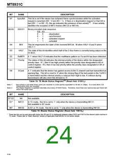
M/S
This bit represents the state of the transmitted M/S-bit. M when HALF=0 and S when
HALF=1.
HALF
The state of this bit identifies which half of the frame will be transmitted on the
S-Bus. The operation of this signal is similar to that of the HALF pin.
TxMFR
RegSel
A ’1’ in this bit, while HALF = 0, will force the transmission of a multiframe sequence in the
Fa and N bits, i.e., Fa=1 and N=0. A ‘0’ will resume normal operation, i.e., Fa=0 and N=1.
If the register select bit is set to ’1’, the control register is redefined as the diagnostic
register. A ’0’ give access to the control register.
(2)
Table 13. NT Mode C-channel Control Register (Write Add. 01000B and B0 = 0)
Note 1:
Note 2:
Allow one ST-BUS frame to input the C-channel and one ST-BUS frame to establish the connection.
The C-channel Control Register is updated once every ST-BUS frame. Therefore, this register should not be written to
more than once per frame, otherwise, the last access will override previous ones.
9-91

 MITEL [ MITEL NETWORKS CORPORATION ]