MT8931C
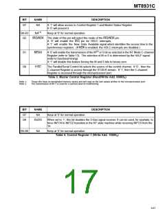
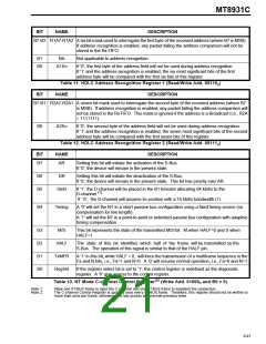
BIT
NAME
DESCRIPTION
B7
NA
A ‘1’ will allow access to Control Register 1 and Master Status Register.
A ‘0’ will prevent it.
(1)
B6-B3
B2
NA
Keep at ’0’ for normal operation.
IRQ/NDA The state of this pin will select the mode of the IRQ/NDA pin.
A ’0’ will enable the IRQ pin for HDLC interrupts.
A ’1’ will enable the New Data Available signal which identifies the access time to the
synchronous registers. (If NDA is enabled, the HDLC interrupts are disabled.)
(2)
B1
B0
M/Sen
P/SC
A ’0’ will enable the transmission of the M or S bit as selected in the NT Mode C-channel
Register (refer to Table 13). The selection of M or S is determined by the HALF signal
(refer to functional timing).
A ’1’ will disable this feature forcing the M and S bits to binary zero.
The Parallel/Serial Control bit selects the source of the control channel. If ’0’, then the
C-channel Register is access through the ST-BUS stream. If ’1’, then the C-channel
Register is accessed through the microprocessor port.
Table 3. Master Control Register (Read/Write Add. 00000B)
Note 1:
Note 2:
These bits have no designated memory space and will read as the last values written to the microprocessor port.
The transmission of M=1 is used for a second level of multiframing.
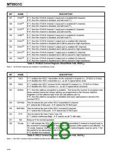
BIT
NAME
DESCRIPTION
B7
B6
NA
Keep at ‘0’ for normal operation.
RxDIS
When set to ‘1’, this bit disables the S-Bus signal receiver. It can be used, for example, to
force INFO4 to INFO2 transition in the NT state machine while receiving INFO3 from the
TE.
B5-B0
NA
Keep at ‘0’ for normal operation.
Table 4. Control Register 1 (Write Add. 10000B)
9-87

 MITEL [ MITEL NETWORKS CORPORATION ]