MT8931C
situation is when the system is trying to synchronize
two nodes of a synchronous network. This allows
multiple TEs to share a common ST-BUS timebase.
The synchronization of the loops is established by
using the clock signals produced by a local TE as an
input timing source to the NT slave.
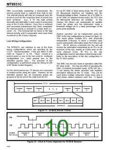
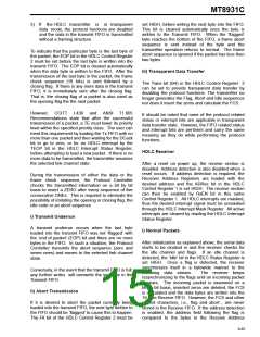
ST-BUS Interface
The ST-BUS is
a
synchronous time division
multiplexed serial bussing scheme with data streams
operating at 2048 kbit/s configured as 32, 64 kbit/s
channels (refer to Fig. 11). Synchroni-zation of the
data transfer is provided from a frame pulse which
identifies the frame boundaries and repeats at an 8
kHz rate. Figure 4 shows how the frame pulse
(F0b) defines the ST-BUS frame boundaries. All
data is clocked into the device on the rising edge of
the 4096 kHz clock (C4b) three quarters of the way
into the bit cell, while data is clocked out on the
falling edge of the 4096 kHz clock at the start of the
bit cell.
Adaptive Timing Operation
On power-up or after a reset, the SNIC in NT mode is
set to operate in fixed timing. To switch to adaptive
timing, the user should:
1) set the DR bit to 1
2) set the Timing bit to 1 in the C-channel
Control Register
All timing signals (i.e. F0b & C4b) are identified as
bidirectional (denoted by the terminating b). The
I/O configuration of these pins is controlled by the
mode of operation (NT or TE). In the NT mode, all
synchronized signals are supplied from an external
source and the SNIC uses this timing while
transferring information to and from the S or
ST-BUS. In the TE mode, an on-board analog
phase-locked loop extracts timing from the received
data on the S-Bus and generates the system
3) wait for 100 ms period
4) proceed in using the AR and DR bits as
desired
Switching from adaptive timing mode is completed
by resetting the Timing bit.
4096 kHz (C4b) and frame pulse (F0b).
The
analog phase-locked loop also maintains proper
phase relation between the timing signals as well as
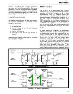
ST-BUS Clock
ST-BUS
Stream
Active on
Channel 0 - 3
Active on
Channels 4 - 7
Active on
Channels 8 - 11
Active on
Channels 12 - 15
MT8931C
NT
MT8931C
NT
MT8931C
NT
MT8931C
NT
System
Frame Pulse
F0b
F0b
F0b
F0b
F0od
F0od
F0od
F0od
to TE
to TE
to TE
to TE
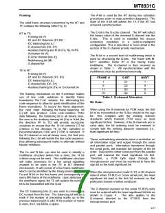
Figure 13 - Daisy Chaining the SNIC
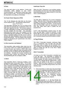
VDD
MT8931C
NT
MT8931C
NT
STAR
F0b
STAR
F0b
System
Frame Pulse
to TE
to TE
DSTi
DSTi
DSTo
Output
ST-BUS Stream
Input
ST-BUS Stream
MT8931C
NT
MT8931C
NT
STAR
F0b
STAR
F0b
to TE
to TE
DSTi
DSTi
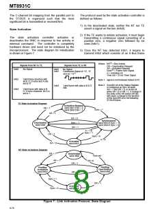
Figure 14 - NT in Star Configuration
9-81

 MITEL [ MITEL NETWORKS CORPORATION ]