MT8931C
The parallel port on the SNIC allows complete
control of the HDLC transceiver and access to all
data, control and status registers. Reading these
registers allows the microprocessor to monitor
HDLC Transceiver
The HDLC Transceiver handles the bit oriented
protocol structure and formats the D-channel as per
level 2 of the X.25 packet switching protocol defined
by CCITT. It transmits and receives the packetized
data (information or control) serially in a format
shown in Figure 15, while providing data
transparency by zero insertion and deletion. It
generates and detects the flags, various link channel
states and the abort sequence. Further, it provides a
cyclic redundancy check on the data packets using
the CCITT defined polynomial. In addition, it can
recognize a single byte, dual byte or an all call
address in the received frame. There is also a
provision to disable the protocol functions and
provide transparent access to either serial port
through the microprocessor port. Other features
provided by the HDLC include, independent port
selection for transmit and received data (e.g.
transmit on S-Bus and receive from ST-BUS),
selectable 16 or 64 kbit/s D-channel as well as an
HDLC loopback from the transmit to the receive port.
These features are enabled through the HDLC
control registers (see Tables 6 and 7).
incoming data on the
S or ST-BUS without
interrupting the normal data flow.
Some registers are classified as asynchronous and
others as synchronous. Synchronous registers are
single-buffered and require synchronous access.
Not all the synchronous registers have the same
access times,
but
all
can be accessed
synchronously in the time during which the NDA
signal is low (refer to Fig. 5). Therefore, it is
recommended that the user make use of the NDA
signal to access these registers.
Since the
synchronous registers use common circuitry, it is
essential that the register be read before being
written. This sequence is important as a write cycle
will overwrite the last data received. These parallel
accesses must be refreshed every frame.
Asynchronous registers, on the other hand, can be
accessed at any time.
The data in TE or NT Mode Status Register,
depending upon the mode selected, is always sent
out on the C-channel of DSTo.
However, in
microprocessor control mode the user can overwrite
this data by writing to the DSTo C-channel Register.
This access can be done anytime outside the frame
pulse interval of the ST-BUS frame. Data written in
the current ST-BUS frame will only appear in the C-
channel of the following frame.
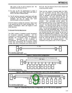
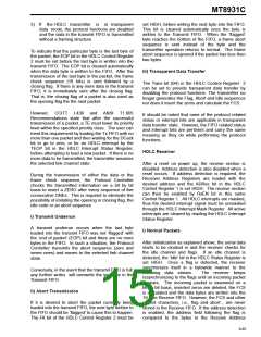
HDLC Frame Format
All frames start with an opening flag and end with a
closing flag as shown in Figure 15. Between these
two flags, a frame contains the data and the frame
check sequence (FCS).
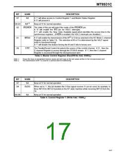
The least significant bit (B0) of the C-channel
Register, selects between the control register or the
diagnostic register. Setting the B0 of the C-channel
Register to ’0’ allow access to the control register.
Setting the LSB of the C-channel Register to ’1’ allow
access to the diagnostic register. The interpretation
of each register is defined in Tables 13 and 14 for NT
mode or Tables 16 and 17 for the TE mode.
FLAG
DATA FIELD
FCS
FLAG
One
Byte
n Bytes
(n ≥ 2)
Two
Bytes
One
Byte
Figure 15 - Frame Format
i) Flag
The flag is a unique pattern of 8 bits (01111110)
defining the frame boundary. The transmit section
generates the flags and appends them automatically
to the frame to be transmitted. The receive section
searches the incoming packets for flags on a
It is important to note that in TE mode, the C-channel
Diagnostic Register should be cleared while the
device is not in the active state (IS0, IS1 ≠ 1,1). This
is accomplished by setting the ClrDia bit of the C-
channel Control Register to 1 until the device is
activated. In serial control mode, the C-channel on
the ST-BUS is loaded into the C-channel Control
Register in every ST-BUS frame; the user should
make sure that a 1 is written to the ClrDia bit in every
frame. However, in parallel control mode the user
needs to set the ClrDia bit only once to keep the
Diagnostic Register cleared. Once full activation is
achieved the Diagnostic Register can be written to in
order to enable the various test functions.
bit-by-bit
basis
and
establishes
frame
synchronization. The flags are used only to identify
and synchronize the received frame and are not
transferred to the FIFO.
9-83

 MITEL [ MITEL NETWORKS CORPORATION ]