ProASIC3 Device Family Overview
User Nonvolatile FlashROM
ProASIC3 devices have 1 kbit of on-chip, user-accessible, nonvolatile FlashROM. The FlashROM can be used in
diverse system applications:
•
•
•
•
•
•
•
•
Internet protocol addressing (wireless or fixed)
System calibration settings
Device serialization and/or inventory control
Subscription-based business models (for example, set-top boxes)
Secure key storage for secure communications algorithms
Asset management/tracking
Date stamping
Version management
The FlashROM is written using the standard ProASIC3 IEEE 1532 JTAG programming interface. The core can be
individually programmed (erased and written), and on-chip AES decryption can be used selectively to securely load
data over public networks (except in the A3P015 and A3P030 devices), as in security keys stored in the FlashROM for
a user design.
The FlashROM can be programmed via the JTAG programming interface, and its contents can be read back either
through the JTAG programming interface or via direct FPGA core addressing. Note that the FlashROM can only be
programmed from the JTAG interface and cannot be programmed from the internal logic array.
The FlashROM is programmed as 8 banks of 128 bits; however, reading is performed on a byte-by-byte basis using a
synchronous interface. A 7-bit address from the FPGA core defines which of the 8 banks and which of the 16 bytes
within that bank are being read. The three most significant bits (MSBs) of the FlashROM address determine the bank,
and the four least significant bits (LSBs) of the FlashROM address define the byte.
The ProASIC3 development software solutions, Libero® System-on-Chip (SoC) and Designer, have extensive support
for the FlashROM. One such feature is auto-generation of sequential programming files for applications requiring a
unique serial number in each part. Another feature allows the inclusion of static data for system version control. Data
for the FlashROM can be generated quickly and easily using Libero SoC and Designer software tools. Comprehensive
programming file support is also included to allow for easy programming of large numbers of parts with differing
FlashROM contents.
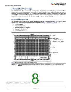
SRAM and FIFO
ProASIC3 devices (except the A3P015 and A3P030 devices) have embedded SRAM blocks along their north and
south sides. Each variable-aspect-ratio SRAM block is 4,608 bits in size. Available memory configurations are 256×18,
512×9, 1k×4, 2k×2, and 4k×1 bits. The individual blocks have independent read and write ports that can be configured
with different bit widths on each port. For example, data can be sent through a 4-bit port and read as a single bitstream.
The embedded SRAM blocks can be initialized via the device JTAG port (ROM emulation mode) using the UJTAG
macro (except in A3P015 and A3P030 devices).
In addition, every SRAM block has an embedded FIFO control unit. The control unit allows the SRAM block to be
configured as a synchronous FIFO without using additional core VersaTiles. The FIFO width and depth are
programmable. The FIFO also features programmable Almost Empty (AEMPTY) and Almost Full (AFULL) flags in
addition to the normal Empty and Full flags. The embedded FIFO control unit contains the counters necessary for
generation of the read and write address pointers. The embedded SRAM/FIFO blocks can be cascaded to create
larger configurations.
PLL and CCC
ProASIC3 devices provide designers with very flexible clock conditioning capabilities. Each member of the ProASIC3
family contains six CCCs. One CCC (center west side) has a PLL. The A3P015 and A3P030 devices do not have a
PLL.
The six CCC blocks are located at the four corners and the centers of the east and west sides.
All six CCC blocks are usable; the four corner CCCs and the east CCC allow simple clock delay operations as well as
clock spine access.
The inputs of the six CCC blocks are accessible from the FPGA core or from one of several inputs located near the
CCC that have dedicated connections to the CCC block.
1-5
Revision 18

 MICROSEMI [ Microsemi ]