1 – ProASIC3 Device Family Overview
General Description
ProASIC3, the third-generation family of Microsemi flash FPGAs, offers performance, density, and
features beyond those of the ProASICPLUS® family. Nonvolatile flash technology gives ProASIC3 devices
the advantage of being a secure, low power, single-chip solution that is Instant On. ProASIC3 is
reprogrammable and offers time-to-market benefits at an ASIC-level unit cost. These features enable
designers to create high-density systems using existing ASIC or FPGA design flows and tools.
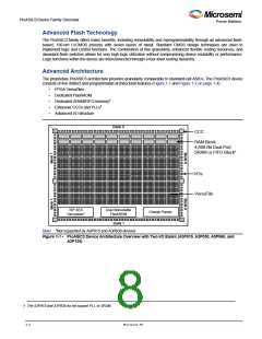
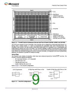
ProASIC3 devices offer 1 kbit of on-chip, reprogrammable, nonvolatile FlashROM storage as well as
clock conditioning circuitry based on an integrated phase-locked loop (PLL). The A3P015 and A3P030
devices have no PLL or RAM support. ProASIC3 devices have up to 1 million system gates, supported
with up to 144 kbits of true dual-port SRAM and up to 300 user I/Os.
ProASIC3 devices support the ARM Cortex-M1 processor. The ARM-enabled devices have Microsemi
ordering numbers that begin with M1A3P (Cortex-M1) and do not support AES decryption.
Flash Advantages
Reduced Cost of Ownership
Advantages to the designer extend beyond low unit cost, performance, and ease of use. Unlike SRAM-
based FPGAs, flash-based ProASIC3 devices allow all functionality to be Instant On; no external boot
PROM is required. On-board security mechanisms prevent access to all the programming information
and enable secure remote updates of the FPGA logic. Designers can perform secure remote in-system
reprogramming to support future design iterations and field upgrades with confidence that valuable
intellectual property (IP) cannot be compromised or copied. Secure ISP can be performed using the
industry-standard AES algorithm. The ProASIC3 family device architecture mitigates the need for ASIC
migration at higher user volumes. This makes the ProASIC3 family a cost-effective ASIC replacement
solution, especially for applications in the consumer, networking/ communications, computing, and
avionics markets.
Security
The nonvolatile, flash-based ProASIC3 devices do not require a boot PROM, so there is no vulnerable
external bitstream that can be easily copied. ProASIC3 devices incorporate FlashLock, which provides a
unique combination of reprogrammability and design security without external overhead, advantages that
only an FPGA with nonvolatile flash programming can offer.
ProASIC3 devices utilize a 128-bit flash-based lock and a separate AES key to provide the highest level
of protection in the FPGA industry for intellectual property and configuration data. In addition, all
FlashROM data in ProASIC3 devices can be encrypted prior to loading, using the industry-leading
AES-128 (FIPS192) bit block cipher encryption standard. The AES standard was adopted by the National
Institute of Standards and Technology (NIST) in 2000 and replaces the 1977 DES standard. ProASIC3
devices have a built-in AES decryption engine and a flash-based AES key that make them the most
comprehensive programmable logic device security solution available today. ProASIC3 devices with
AES-based security provide a high level of protection for remote field updates over public networks such
as the Internet, and are designed to ensure that valuable IP remains out of the hands of system
overbuilders, system cloners, and IP thieves.
ARM-enabled ProASIC3 devices do not support user-controlled AES security mechanisms. Since the
ARM core must be protected at all times, AES encryption is always on for the core logic, so bitstreams
are always encrypted. There is no user access to encryption for the FlashROM programming data.
Security, built into the FPGA fabric, is an inherent component of the ProASIC3 family. The flash cells are
located beneath seven metal layers, and many device design and layout techniques have been used to
make invasive attacks extremely difficult. The ProASIC3 family, with FlashLock and AES security, is
unique in being highly resistant to both invasive and noninvasive attacks.
Revision 18
1-1

 MICROSEMI [ Microsemi ]