ProASIC3 Flash Family FPGAs
The CCC block has these key features:
•
•
•
•
•
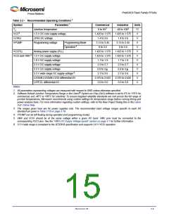
Wide input frequency range (fIN_CCC) = 1.5 MHz to 350 MHz
Output frequency range (fOUT_CCC) = 0.75 MHz to 350 MHz
Clock delay adjustment via programmable and fixed delays from –7.56 ns to +11.12 ns
2 programmable delay types for clock skew minimization
Clock frequency synthesis (for PLL only)
Additional CCC specifications:
•
Internal phase shift = 0°, 90°, 180°, and 270°. Output phase shift depends on the output divider configuration
(for PLL only).
•
•
Output duty cycle = 50% ± 1.5% or better (for PLL only)
Low output jitter: worst case < 2.5% × clock period peak-to-peak period jitter when single global network used
(for PLL only)
•
•
•
•
Maximum acquisition time = 300 µs (for PLL only)
Low power consumption of 5 mW
Exceptional tolerance to input period jitter— allowable input jitter is up to 1.5 ns (for PLL only)
Four precise phases; maximum misalignment between adjacent phases of 40 ps × (350 MHz / fOUT_CCC) (for
PLL only)
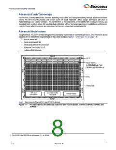
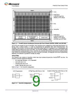
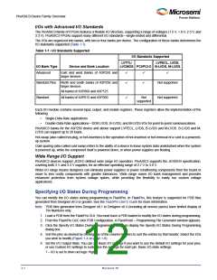
Global Clocking
ProASIC3 devices have extensive support for multiple clocking domains. In addition to the CCC and PLL support
described above, there is a comprehensive global clock distribution network.
Each VersaTile input and output port has access to nine VersaNets: six chip (main) and three quadrant global
networks. The VersaNets can be driven by the CCC or directly accessed from the core via multiplexers (MUXes). The
VersaNets can be used to distribute low-skew clock signals or for rapid distribution of high fanout nets.
Revision 18
1-6

 MICROSEMI [ Microsemi ]