2 – ProASIC3 DC and Switching Characteristics
General Specifications
Operating Conditions
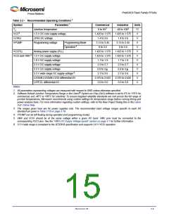
Stresses beyond those listed in Table 2-1 may cause permanent damage to the device.
Exposure to absolute maximum rating conditions for extended periods may affect device reliability.
Absolute Maximum Ratings are stress ratings only; functional operation of the device at these or any
other conditions beyond those listed under the Recommended Operating Conditions specified in
Table 2-2 on page 2-2 is not implied.
Table 2-1 • Absolute Maximum Ratings
Symbol
VCC
Parameter
DC core supply voltage
JTAG DC voltage
Limits
Units
–0.3 to 1.65
–0.3 to 3.75
–0.3 to 3.75
–0.3 to 1.65
–0.3 to 3.75
–0.3 to 3.75
V
V
V
V
V
V
V
VJTAG
VPUMP Programming voltage
VCCPLL Analog power supply (PLL)
VCCI
VMV
VI
DC I/O output buffer supply voltage
DC I/O input buffer supply voltage
I/O input voltage
–0.3 V to 3.6 V
(when I/O hot insertion mode is enabled)
–0.3 V to (VCCI + 1 V) or 3.6 V, whichever voltage is lower
(when I/O hot-insertion mode is disabled)
2
TSTG
Storage temperature
Junction temperature
–65 to +150
+125
°C
°C
2
TJ
Notes:
1. The device should be operated within the limits specified by the datasheet. During transitions, the input signal may
undershoot or overshoot according to the limits shown in Table 2-4 on page 2-3.
2. VMV pins must be connected to the corresponding VCCI pins. See the "VMVx I/O Supply Voltage (quiet)" section on
page 3-1 for further information.
3. For flash programming and retention maximum limits, refer to Table 2-3 on page 2-3, and for recommended operating
limits, refer to Table 2-2 on page 2-2.
Revision 18
2-1

 MICROSEMI [ Microsemi ]