ProASIC3 Flash Family FPGAs
Bank 0
CCC
RAM Block
4,608-Bit Dual-Port
SRAM or FIFO Block
I/Os
VersaTile
RAM Block
4,608-Bit Dual-Port
SRAM or FIFO Block
(A3P600 and A3P1000)
ISP AES
Decryption
User Nonvolatile
FlashROM
Charge Pumps
Bank 2
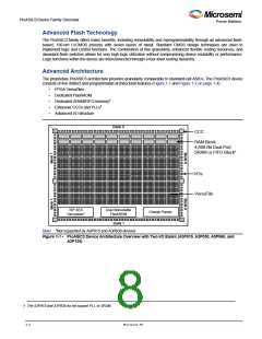
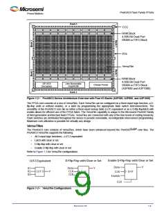
Figure 1-2 • ProASIC3 Device Architecture Overview with Four I/O Banks (A3P250, A3P600, and A3P1000)
The FPGA core consists of a sea of VersaTiles. Each VersaTile can be configured as a three-input logic function, a D-
flip-flop (with or without enable), or a latch by programming the appropriate flash switch interconnections. The
versatility of the ProASIC3 core tile as either a three-input lookup table (LUT) equivalent or as a D-flip-flop/latch with
enable allows for efficient use of the FPGA fabric. The VersaTile capability is unique to the Microsemi ProASIC family
of third-generation architecture flash FPGAs. VersaTiles are connected with any of the four levels of routing hierarchy.
Flash switches are distributed throughout the device to provide nonvolatile, reconfigurable interconnect programming.
Maximum core utilization is possible for virtually any design.
VersaTiles
The ProASIC3 core consists of VersaTiles, which have been enhanced beyond the ProASICPLUS® core tiles. The
ProASIC3 VersaTile supports the following:
•
•
•
•
All 3-input logic functions—LUT-3 equivalent
Latch with clear or set
D-flip-flop with clear or set
Enable D-flip-flop with clear or set
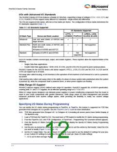
Refer to Figure 1-3 for VersaTile configurations.
Enable D-Flip-Flop w ith Clear or Set
D-Flip-Flop w ith Clear or Set
LUT-3 Equivalent
X1
Data
Y
Data
CLK
CLR
Y
X2
X3
LUT-3
Y
D-FF
CLK
D-FF
Enable
CLR
Figure 1-3 • VersaTile Configurations
Revision 18
1-4

 MICROSEMI [ Microsemi ]