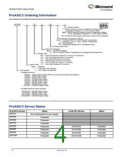
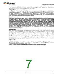
ProASIC3 Device Family Overview
Advanced Flash Technology
The ProASIC3 family offers many benefits, including nonvolatility and reprogrammability through an advanced flash-
based, 130-nm LVCMOS process with seven layers of metal. Standard CMOS design techniques are used to
implement logic and control functions. The combination of fine granularity, enhanced flexible routing resources, and
abundant flash switches allows for very high logic utilization without compromising device routability or performance.
Logic functions within the device are interconnected through a four-level routing hierarchy.
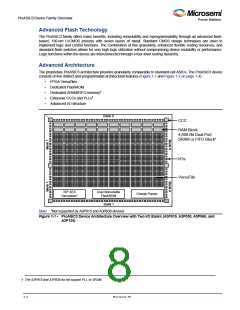
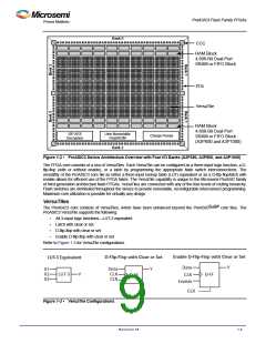
Advanced Architecture
The proprietary ProASIC3 architecture provides granularity comparable to standard-cell ASICs. The ProASIC3 device
consists of five distinct and programmable architectural features (Figure 1-1 and Figure 1-2 on page 1-4):
•
•
•
•
•
FPGA VersaTiles
Dedicated FlashROM
Dedicated SRAM/FIFO memory†
Extensive CCCs and PLLs†
Advanced I/O structure
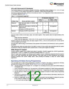
Bank 0
CCC
RAM Block
4,608-Bit Dual-Port
SRAM or FIFO Block*
I/Os
VersaTile
ISP AES
Decryption*
User Nonvolatile
FlashROM
Charge Pumps
Bank 1
Note: *Not supported by A3P015 and A3P030 devices
Figure 1-1 • ProASIC3 Device Architecture Overview with Two I/O Banks (A3P015, A3P030, A3P060, and
A3P125)
† The A3P015 and A3P030 do not support PLL or SRAM.
1-3
Revision 18

 MICROSEMI [ Microsemi ]