ProASIC3 Device Family Overview
I/Os with Advanced I/O Standards
The ProASIC3 family of FPGAs features a flexible I/O structure, supporting a range of voltages (1.5 V, 1.8 V, 2.5 V, and
3.3 V). ProASIC3 FPGAs support many different I/O standards—single-ended and differential.
The I/Os are organized into banks, with two or four banks per device. The configuration of these banks determines the
I/O standards supported (Table 1-1).
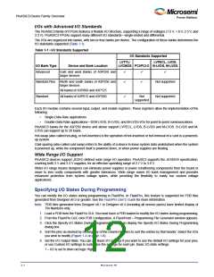
Table 1-1 • I/O Standards Supported
I/O Standards Supported
LVTTL/
LVPECL, LVDS,
I/O Bank Type
Device and Bank Location
LVCMOS PCI/PCI-X B-LVDS, M-LVDS
Advanced
East and west Banks of A3P250 and
larger devices
Standard Plus
Standard
North and south banks of A3P250 and
larger devices
Not supported
All banks of A3P060 and A3P125
All banks of A3P015 and A3P030
Not
supported
Not supported
Each I/O module contains several input, output, and enable registers. These registers allow the implementation of the
following:
•
•
Single-Data-Rate applications
Double-Data-Rate applications—DDR LVDS, B-LVDS, and M-LVDS I/Os for point-to-point communications
ProASIC3 banks for the A3P250 device and above support LVPECL, LVDS, B-LVDS and M-LVDS. B-LVDS and M-
LVDS can support up to 20 loads.
Hot-swap (also called hot-plug, or hot-insertion) is the operation of hot-insertion or hot-removal of a card in a powered-
up system.
Cold-sparing (also called cold-swap) refers to the ability of a device to leave system data undisturbed when the system
is powered up, while the component itself is powered down, or when power supplies are floating.
Wide Range I/O Support
ProASIC3 devices support JEDEC-defined wide range I/O operation. ProASIC3 supports the JESD8-B specification,
covering both 3 V and 3.3 V supplies, for an effective operating range of 2.7 V to 3.6 V.
Wider I/O range means designers can eliminate power supplies or power conditioning components from the board or
move to less costly components with greater tolerances. Wide range eases I/O bank management and provides
enhanced protection from system voltage spikes, while providing the flexibility to easily run custom voltage
applications.
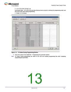
Specifying I/O States During Programming
You can modify the I/O states during programming in FlashPro. In FlashPro, this feature is supported for PDB files
generated from Designer v8.5 or greater. See the FlashPro User’s Guide for more information.
Note: PDB files generated from Designer v8.1 to Designer v8.4 (including all service packs) have limited display of
Pin Numbers only.
1. Load a PDB from the FlashPro GUI. You must have a PDB loaded to modify the I/O states during programming.
2. From the FlashPro GUI, click PDB Configuration. A FlashPoint – Programming File Generator window appears.
3. Click the Specify I/O States During Programming button to display the Specify I/O States During Programming
dialog box.
4. Sort the pins as desired by clicking any of the column headers to sort the entries by that header. Select the I/Os
you wish to modify (Figure 1-4 on page 1-8).
5. Set the I/O Output State. You can set Basic I/O settings if you want to use the default I/O settings for your pins,
or use Custom I/O settings to customize the settings for each pin. Basic I/O state settings:
1 – I/O is set to drive out logic High
1-7
Revision 18

 MICROSEMI [ Microsemi ]