‡
Pre lim in a ry
MT9V012 - 1/6-In ch VGA CMOS Dig it a l Im a g e Se n so r
Re g ist e rs
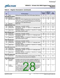
Ta b le 6: Re g ist e r De scrip t io n (co n t in u e d )
Syn c’d
De fa u lt t o Fra m e
Ba d
Fra m e
Bit
Bit De scrip t io n
(h e x)
St a rt
0x0A (10) Ro w Sp e e d
2:
1
Y
YM
Pixel Clock
Speed
A programmed value of N gives a pixel clock period of (2 x N)
master clocks. A value of 0 is treated like (and reads back as)
a value of 1.
3
0
1
N
N
N
N
Reserved
Read-only.
7:4
Delay Pixel
Clock
Number of half-master-clock-cycle increments to delay the
rising edge of PIXCLK relative to transitions on
FRAME_VALID, LINE_VALID, and DOUT.
8
0
N
N
Invert Pixel
Clock
Invert PIXCLK. When clear, FRAME_VALID, LINE_VALID, and
DOUT are set up relative to the delayed rising edge of
PIXCLK. When set, FRAME_VALID, LINE_VALID, and DOUT are
set up relative to the delayed falling edge of PIXCLK.
13
0
0
Reserved
Reserved
Reserved. Do not change from default value.
Reserved. Do not change from default value.
15:14
0x0B (11) Ext ra De la y
13:0
0
Y
Y
Extra Delay
Extra blanking inserted between frames. A programmed
value of N increases the vertical blanking time by N pixel
clock periods. Can be used to get a more exact frame rate.
May affect the integration times of parts of the image when
the integration time is less than 1 frame.
0x0C (12) Sh u t t e r De la y
10:0
0
N
Shutter Delay
The amount of time from the end of the sampling sequence
to the beginning of the pixel reset sequence. This register
should normally be set to zero. A non-zero value will only
have a visible effect on the image when the integration time
(Reg0x09) is small. A programmed value of N reduces the
integration time by N master clock periods (N / 2) pixel clock
periods). Legal values for this register are shown in
"Maximum Shutter Delay" on page 37.
0x0D (13) Re se t
0
0
N
YM
Reset
Setting this bit puts the sensor into reset; the frame being
generated will be truncated, and the signal interface will go
to an idle state. All internal registers (except for this bit) will
go to the default power-up state. Clearing this bit resumes
normal operation.
1
2
0
0
N
N
YM
YM
Restart
Setting this bit causes the sensor to truncate the current
frame and start resetting the first row. The delay before the
first valid frame is read out equals the integration time. This
bit is write-1, but always reads back as “0.”
Standby
Reserved
Setting this bit places the sensor in a low-power state. See
“Power Saving Modes” on page 42.
3
4
0
0
N
N
N
N
This read/write bit has no function.
Output Disable Setting this bit puts the signal interface into High-Z. See
“Output Enable Control” on page 41.
5
6
0
0
Reserved
Reserved.
N
N
Drive outputs
By default, asserting STANDBY causes the signal interface to
enter High-Z. Setting this bit stops STANDBY from
contributing to output-enable control. See “Output Enable
Control” on page 41.
PDF: 814eb99f/Source: 8175e929
MT9V012_2.fm - Rev. B 2/05 EN
Micron Technology, Inc., reserves the right to change products or specifications without notice.
©2004 Micron Technology, Inc. All rights reserved.
24

 MICRON [ MICRON TECHNOLOGY ]