‡
Pre lim in a ry
MT9V012 - 1/6-In ch VGA CMOS Dig it a l Im a g e Se n so r
Re g ist e rs
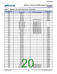
Ta b le 5: Re g ist e r List a n d De fa u lt Va lu e (co n t in u e d )
Re g ist e r Nu m b e r
(He x)
De fa u lt Va lu e
(He x)
De scrip t io n
Da t a Fo rm a t (Bin a ry)
0xF5
0xF6
0xF7
0xF8
0xF9
0xFA
0xFB
0xFC
0xFD
0xFF
Reserved
Reserved
Reserved
Reserved
Reserved
Reserved
Reserved
Reserved
Reserved
Chip Version
—
0x03FF
0x01FF
0x0000
0x0000
0x0000
0x0000
0x0000
0x0000
0x0000
0x1222
—
—
—
—
—
—
—
—
0001 0010 0010 0010
Note:
1 = always 1
0 = always 0
d = programmable
? = read-only
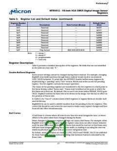
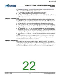
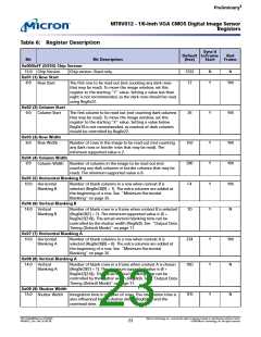
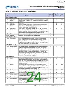
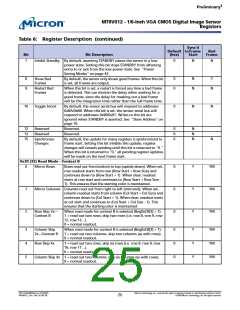
Re g ist e r De scrip t io n
Table 6 provides a detailed description of the registers. Bit fields that are not identified
in the table are read-only “0.”
Do u b le -Bu ffe re d Re g ist e rs
Some sensor settings cannot be changed during frame readout. For example, changing
Reg0x03 (row width) partway through frame readout would result in inconsistent
LINE_VALID behavior. To avoid this, the MT9V012 double buffers many registers by
implementing a “pending” and a “live” version. Reads and writes access the pending
register. The live register controls the sensor operation.
The values in the pending registers are transferred to the live registers at a fixed point in
the frame timing, called “frame start.” Frame start is defined as the point at which the
first dark row is read out. By default, this occurs 6 row times before FRAME_VALID goes
HIGH. Reg0x22 enables the dark rows to be shown in the image, but this has no effect on
the position of frame start.
In Table 6, the “Sync’d” column shows which registers or register fields are double-buff-
ered in this way.
Reg0x0D[15] can be used to inhibit transfers from the pending to the live registers. This
control bit should be used when the user wants to make many register changes and have
them all take effect simultaneously.
Ba d Fra m e s
A bad frame is a frame where all rows do not have the same integration time, or where
offsets to the pixel values have changed during the frame.
Many changes to the sensor register settings can cause a bad frame. For example, when
Reg0x03 (row width) is changed, the new register value does not affect sensor behavior
until the next frame start. However, the frame that would be read out at that frame start
will have been integrated using the old row width, so reading it out using the new row
width would result in a frame with an incorrect integration time.
By default, most bad frames are masked: LINE_VALID and FRAME_VALID are inhibited
for these frames so that the vertical blanking time between frames is extended by the
frame time.
PDF: 814eb99f/Source: 8175e929
MT9V012_2.fm - Rev. B 2/05 EN
Micron Technology, Inc., reserves the right to change products or specifications without notice.
21
©2004 Micron Technology, Inc. All rights reserved.

 MICRON [ MICRON TECHNOLOGY ]