‡
Pre lim in a ry
MT9V012 - 1/6-In ch VGA CMOS Dig it a l Im a g e Se n so r
Tw o -Wire Se ria l In t e rfa ce Sa m p le Writ e a n d Re a d Se q u e n ce s
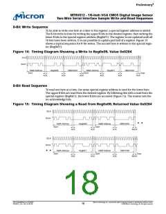
8-Bit Writ e Se q u e n ce
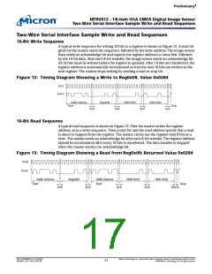
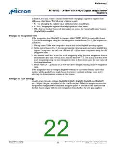
To be able to write one byte at a time to the register, a special register address is added.
The 8-bit write is done by writing the upper 8 bits to the desired register, then writing the
lower 8 bits to the special register address (Reg0xF1). The register is not updated until all
16 bits have been written. It is not possible to update just half of a register. Figure 14
shows a typical sequence for 8-bit writes. The second byte is written to the special regis-
ter (Reg0xF1).
Fig u re 14: Tim in g Dia g ra m Sh o w in g a Writ e t o Re g 0x09, Va lu e 0x0284
SCLK
SDATA
0xBA Address
Start
Reg0x09
0000 0010
0xBA Address
Start
Reg0xF1
1000 0100
Stop
ACK
ACK
ACK
ACK
ACK
ACK
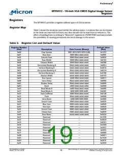
8-Bit Re a d Se q u e n ce
To read one byte at a time, the same special register address is used for the lower byte.
The upper 8 bits are read from the desired register. By following this with a read from the
special register (Reg0xF1), the lower 8 bits are accessed (Figure 15). The master sets the
no-acknowledge bits.
Fig u re 15: Tim in g Dia g ra m Sh o w in g a Re a d fro m Re g 0x09; Re t u rn e d Va lu e 0x0284
SCLK
SDATA
0xBA Address
Start
Reg0x09
0xBB Address
Start
• •
0000 0010
ACK
ACK
ACK
NACK
SCLK
SDATA
0xBA Address
Start
Reg0xF1
0xBB Address
Start
1000 0100
• •
Stop
NACK
ACK
ACK
ACK
PDF: 814eb99f/Source: 8175e929
MT9V012_2.fm - Rev. B 2/05 EN
Micron Technology, Inc., reserves the right to change products or specifications without notice.
©2004 Micron Technology, Inc. All rights reserved.
18

 MICRON [ MICRON TECHNOLOGY ]