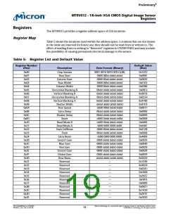
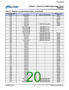
‡
Pre lim in a ry
MT9V012 - 1/6-In ch VGA CMOS Dig it a l Im a g e Se n so r
Tw o -Wire Se ria l In t e rfa ce Sa m p le Writ e a n d Re a d Se q u e n ce s
Tw o -Wire Se ria l In t e rfa ce Sa m p le Writ e a n d Re a d Se q u e n ce s
16-Bit Writ e Se q u e n ce
A typical write sequence for writing 16 bits to a register is shown in Figure 12. A start bit
given by the master starts the sequence, followed by the write address. The image sensor
then sends an acknowledge bit and expects the register address to come first, followed
by the 16-bit data. After each 8-bit transfer, the image sensor sends an acknowledge bit.
All 16 bits must be written before the register is updated. After 16 bits are transferred, the
register address is automatically incremented so that the next 16 bits are written to the
next register. The master stops writing by sending a start or stop bit.
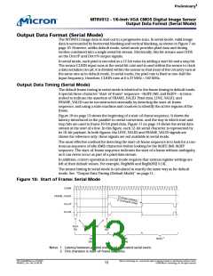
Fig u re 12: Tim in g Dia g ra m Sh o w in g a Writ e t o Re g 0x09, Va lu e 0x0284
SCLK
SDATA
0xBA Address
Start
Reg0x09
0000 0010
1000 0100
Stop
ACK
ACK
ACK
ACK
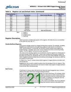
16-Bit Re a d Se q u e n ce
A typical read sequence is shown in Figure 13. First the master writes the register
address, as in a write sequence. Then a start bit and the read address specify that a read
is about to happen from the register. The master clocks out the register data 8 bits at a
time. The master sends an acknowledge bit after each 8-bit transfer. The register address
should be incremented after every 16 bits is transferred. The data transfer is stopped
when the master sends a no-acknowledge bit.
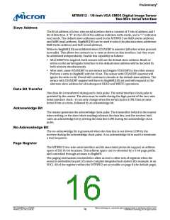
Fig u re 13: Tim in g Dia g ra m Sh o w in g a Re a d fro m Re g 0x09; Re t u rn e d Va lu e 0x0284
SCLK
SDATA
0xBA Address
Start
Reg0x09
0xBB Address
Start
0000 0010
1000 0100
Stop
ACK
ACK
ACK
ACK
NACK
PDF: 814eb99f/Source: 8175e929
MT9V012_2.fm - Rev. B 2/05 EN
Micron Technology, Inc., reserves the right to change products or specifications without notice.
©2004 Micron Technology, Inc. All rights reserved.
17

 MICRON [ MICRON TECHNOLOGY ]