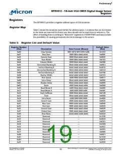
‡
Pre lim in a ry
MT9V012 - 1/6-In ch VGA CMOS Dig it a l Im a g e Se n so r
Tw o -Wire Se ria l In t e rfa ce
Tw o -Wire Se ria l In t e rfa ce
The two-wire serial register interface enables read/ write access to control and status
registers within the MT9V012.
The interface protocol uses a master/ slave model in which a master controls one or
more slave devices. The sensor acts as a slave device. The master generates a clock
(SCLK) that is an input to the sensor and used to synchronize transfers. Data is trans-
ferred between the master and the slave on a bidirectional signal (SDATA). The SDATA sig-
nal is pulled up to VDD off-chip by a 1.5KΩ resistor. Either the slave or master device can
drive the SDATA line LOW—the interface protocol determines which device is allowed to
drive the SDATA line at any given time.
Pro t o co l
The two-wire serial interface defines several different transmission codes, as follows:
• a start bit
• the slave device 8-bit address
• a(an) (no) acknowledge bit
• an 8-bit message
• a stop bit
Se q u e n ce
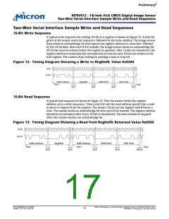
A typical read or write sequence begins by the master sending a start bit. After the start
bit, the master sends the 8-bit slave-device address. The last bit of the address deter-
mines if the request will be a read or a write, where a “0” indicates a write and a “1” indi-
cates a read. The slave device acknowledges receipt of the address by sending an
acknowledge bit back to the master.
If the request was a write, the master then transfers the 8-bit register address to which a
write should take place. The slave sends an acknowledge bit to indicate that the register
address has been received. The master then transfers the data, 8 bits at a time, with the
slave sending an acknowledge bit after each 8 bits. The MT9V012 uses 16-bit data for its
internal registers, thus requiring two 8-bit transfers to write to one register. After 16 bits
are transferred, the register address is automatically incremented, so that the next 16
bits are written to the next register address. The master stops writing by sending a start
or stop bit.
A typical read sequence is executed as follows. The master sends the write mode slave
address and 8-bit register address, just as in the write request. The master then sends a
start bit and the read mode slave address, and clocks out the register data, 8 bits at a
time. The master sends an acknowledge bit after each 8-bit transfer. The register address
is auto-incremented after every 16 bits is transferred. The data transfer is stopped when
the master sends a no-acknowledge bit.
Bu s Id le St a t e
The bus is idle when both the data and clock lines are HIGH. Control of the bus is initi-
ated with a start bit, and the bus is released with a stop bit. Only the master can generate
the start and stop bits.
St a rt Bit
St o p Bit
The start bit is defined as a HIGH-to-LOW data line transition while the clock line is
HIGH.
The stop bit is defined as a LOW-to-HIGH data line transition while the clock line is
HIGH.
PDF: 814eb99f/Source: 8175e929
MT9V012_2.fm - Rev. B 2/05 EN
Micron Technology, Inc., reserves the right to change products or specifications without notice.
15
©2004 Micron Technology, Inc. All rights reserved.

 MICRON [ MICRON TECHNOLOGY ]