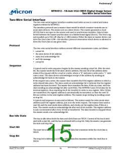
‡
Pre lim in a ry
MT9V012 - 1/6-In ch VGA CMOS Dig it a l Im a g e Se n so r
Ou t p u t Da t a Fo rm a t (De fa u lt Mo d e )
Ou t p u t Da t a Tim in g (De fa u lt Mo d e )
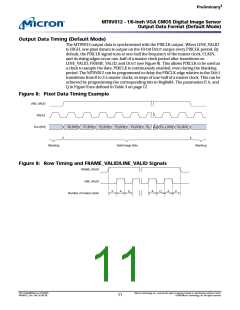
The MT9V012 output data is synchronized with the PIXCLK output. When LINE_VALID
is HIGH, one pixel datum is output on the 10-bit DOUT output every PIXCLK period. By
default, the PIXCLK signal runs at one-half the frequency of the master clock, CLKIN,
and its rising edges occur one-half of a master clock period after transitions on
LINE_VALID, FRAME_VALID, and DOUT (see Figure 8). This allows PIXCLK to be used as
a clock to sample the data. PIXCLK is continuously enabled, even during the blanking
period. The MT9V012 can be programmed to delay the PIXCLK edge relative to the DOUT
transitions from 0 to 3.5 master clocks, in steps of one-half of a master clock. This can be
achieved by programming the corresponding bits in Reg0x0A. The parameters P, A, and
Q in Figure 9 are defined in Table 3 on page 12.
Fig u re 8: Pixe l Da t a Tim in g Exa m p le
LINE_VALID
PIXCLK
P
0
[9:0]
P
1
[9:0]
P
2
[9:0]
P
3
[9:0]
P
4
[9:0]
P
5
P
P
[9:0]
P [9:0]
n
DOUT[9:0]
n-2 n-1
Blanking
Valid Image Data
Blanking
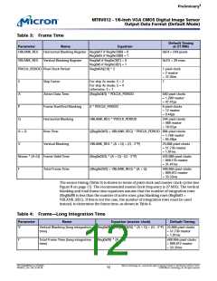
Fig u re 9: Ro w Tim in g a n d FRAME_VALID/LINE_VALID Sig n a ls
FRAME_VALID
LINE_VALID
P
A
Q
A
Q
A
P
Number of master clocks
PDF: 814eb99f/Source: 8175e929
MT9V012_2.fm - Rev. B 2/05 EN
Micron Technology, Inc., reserves the right to change products or specifications without notice.
©2004 Micron Technology, Inc. All rights reserved.
11

 MICRON [ MICRON TECHNOLOGY ]