ADVANCE
4 MEG x 8, 4 MEG x 9, 2 MEG x 18, 1 MEG x 36
1.8V VDD, HSTL, QDRIIb2 SRAM
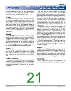
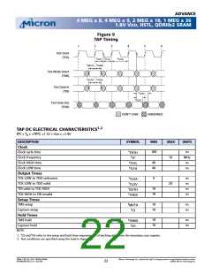
Figure 9
TAP Timing
1
2
3
4
5
6
Test Clock
(TCK)
t
t
t
t
THTH
THTL
TLTH
t
t
MVTH
DVTH
THMX
Test Mode Select
(TMS)
t
THDX
Test Data-In
(TDI)
t
TLOV
t
TLOX
Test Data-Out
(TDO)
DON’T CARE
UNDEFINED
TAP DC ELECTRICAL CHARACTERISTICS1,2
0ºC
?
TA
?
+70ºC; +1.7V ? VDD ? +1.9V
DESCRIPTION
SYMBOL
MIN
MAX
UNITS
Clock
tTHTH
fTF
tTHTL
tTLTH
100
ns
MHz
ns
Clock cycle time
Clock frequency
Clock HIGH time
Clock LOW time
10
40
40
ns
Output Times
tTLOX
tTLOV
tDVTH
tTHDX
0
ns
ns
ns
ns
TCK LOW to TDO unknown
20
TCK LOW to TDO valid
TDI valid to TCK HIGH
TCK HIGH to TDI invalid
10
10
Setup Times
tMVTH
tCS
TMS setup
10
10
ns
ns
Capture setup
Hold Times
tTHMX
tCH
TMS hold
10
10
ns
ns
Capture hold
NOTE:
t
t
1. CS and CH refer to the setup and hold time requirements of latching data from the boundary scan register.
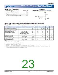
2. Test conditions are specified using the load in Figure 10.
36Mb: 1.8V VDD, HSTL, QDRIIb2 SRAM
MT54W2MH18B_A.fm - Rev 9/02
Micron Technology, Inc., reserves the right to change products or specifications without notice.
©2002, Micron Technology Inc.
22

 MICRON [ MICRON TECHNOLOGY ]