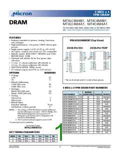
4 MEG x 4
FPM DRAM
GENERALDESCRIPTION
Th e 4 Meg x 4 DRAM is a ran dom ly accessed, solid-
state m em ory con tain in g 16,777,216 bits organ ized in
a x4 con figuration . RAS# is used to latch th e row
address (first 11 bits for 2K an d first 12 bits for 4K). On ce
th e page h as been open ed by RAS#, CAS# is used to latch
th e colum n address (th e latter 11 bits for 2K an d th e
latter 10 bits for 4K; address pin s A10 an d A11 are “Don ’t
Care”).
Addition al colum n s m ay be accessed by providin g valid
colum n addresses, strobin g CAS# an d h oldin g RAS#
LOW, th us executin g faster m em ory cycles. Return in g
RAS# HIGH term in ates th e page m ode of operation ,
i.e., closes th e page.
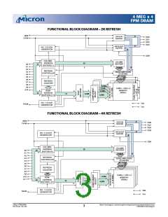
DRAM REFRESH
Preserve correct m em ory cell data by m ain tain in g
power an d executin g an y RAS# cycle (READ, WRITE)
or RAS# REFRESH cycle (RAS#-ONLY, CBR, or HID-
DEN) so th at all com bin ation s of RAS# addresses (2,048
for 2K an d 4,096 for 4K) are executed with in tREF
(MAX), regardless of sequen ce. Th e CBR an d SELF
REFRESH cycles will in voke th e in tern al refresh coun ter
for autom atic RAS# addressin g.
READ an d WRITE cycles are selected with th e WE#
in put. A logic HIGH on WE# dictates read m ode, wh ile
a logic LOW on WE# dictates write m ode. Durin g a
WRITE cycle, data-in (D) is latch ed by th e fallin g edge
of WE# or CAS#, wh ich ever occurs last. If WE# goes
LOW prior to CAS# goin g LOW, th e output pin s
rem ain open (High - Z) un til th e n ext CAS# cycle,
regardless of OE#.
A logic HIGH on WE# dictates read m ode, wh ile a
logic LOW on WE# dictates write m ode. Durin g a
WRITE cycle, data-in (D) is latch ed by th e fallin g edge
of WE# or CAS#, wh ich ever occurs last. An EARLY
WRITE occurs wh en WE# is taken LOW prior to CAS#
fallin g. A LATE WRITE or READ-MODIFY-WRITE
occurs wh en WE# falls after CAS# is taken LOW. Durin g
EARLY WRITE cycles, th e data outputs (Q) will rem ain
High -Z regardless of th e state of OE#. Durin g LATE
WRITE or READ-MODIFY-WRITE cycles, OE# m ust be
taken HIGH to disable th e data outputs prior to
applyin g in put data. If a LATE WRITE or READ-
MODIFY-WRITE is attem pted wh ile keepin g OE# LOW,
n o WRITE will occur, an d th e data outputs will drive
read data from th e accessed location .
An option al self refresh m ode is also available th e
“S” version . Th e self refresh feature is in itiated by
perform in g a CBR REFRESH cycle an d h oldin g RAS#
t
LOW for th e specified RASS. Th e “S” option allows th e
user th e ch oice of a fully static, low-power data reten -
tion m ode or a dyn am ic refresh m ode at th e exten ded
refresh period of 128m s, or 31.25µs per row for a 4K
refresh an d 62.5µs per row for a 2K refresh , wh en usin g
a distributed CBR REFRESH. Th is refresh rate can be
applied durin g n orm al operation , as well as durin g a
stan dby or battery backup m ode.
Th e self refresh m ode is term in ated by drivin g RAS#
HIGH for a m in im um tim e of tRPS. Th is delay allows for
th e com pletion of an y in tern al refresh cycles th at m ay
be in process at th e tim e of th e RAS# LOW-to-HIGH
tran sition . If th e DRAM con troller uses a distributed
CBR refresh sequen ce, a burst refresh is n ot required
upon exitin g self refresh . However, if th e DRAM con -
troller utilizes RAS#-ONLY or burst CBR refresh se-
quen ce, all rows m ust be refresh ed with a refresh rate of
tRC m in im um prior to resum in g n orm al operation .
Th e four data in puts an d th e four data outputs are
routed th rough four pin s usin g com m on I/O, an d pin
direction is con trolled by WE# an d OE#.
Th e MT4LC4M4B1 an d MT4LC4M4A1 m ust be
refresh ed periodically in order to retain stored data.
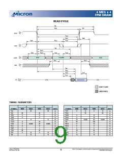
FAST PAGE MODE ACCESS
STANDBY
Page operation s allow faster data operation s (READ,
W RITE or READ-MODIFY-W RITE) with in a row-
address-defin ed page boun dary. Th e page cycle is al-
ways in itiated with a row address strobed in by RAS#,
followed by a colum n address strobed in by CAS#.
Return in g RAS# an d CAS# HIGH term in ates a
m em ory cycle an d decreases ch ip curren t to a reduced
stan dby level. Th e ch ip is precon dition ed for th e n ext
cycle durin g th e RAS# HIGH tim e.
4 Meg x 4 FPM DRAM
D49_5V.p65 – Rev. 5/00
Micron Technology, Inc., reservesthe right to change productsor specificationswithout notice.
©2000, Micron Technology, Inc.
2

 MICRON [ MICRON TECHNOLOGY ]