2 MEG x 16
ASYNC/PAGE/BURST FLASH MEMORY
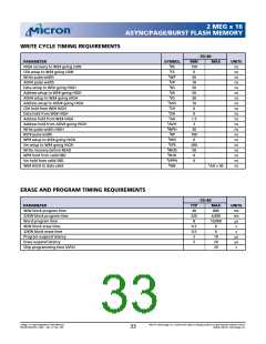
WRITE CYCLE TIMING REQUIREMENTS
-70/-80
PARAMETER
SYMBOL
MIN
150
0
50
10
50
50
50
10
0
0
1.5
3
30
100
0
200
50
0
MAX
UNITS
ns
ns
ns
ns
ns
ns
ns
ns
ns
ns
ns
ns
ns
ns
ns
ns
ns
ns
ns
ns
t
HIGH recovery to WE# going LOW
CE# setup to WE# going LOW
Write pulse width
RS
CS
t
t
WP
VP
DS
AS
t
ADV# pulse width
t
Data setup to WE# going HIGH
Address setup to WE# going HIGH
ADV# setup to WE# going HIGH
Address setup to ADV# going HIGH
CE# hold from WE# HIGH
Data hold from WE# HIGH
Address hold from WE# HIGH
Address hold from ADV# going HIGH
Write pulse width HIGH
t
t
VS
t
AVS
CH
DH
AH
t
t
t
t
AVH
t
WPH
t
RST# pulse width
RP
t
WP# setup to WE# going HIGH
VPP setup to WE# going HIGH
Write recovery before READ
WP# hold from valid SRD
VPP hold from valid SRD
RHS
VPS
t
t
WOS
RHH
t
t
VPPH
0
t
t
WE# HIGH to data valid
WB
AA + 50
ERASE AND PROGRAM TIMING REQUIREMENTS
-70/-80
PARAMETER
TYP
40
320
8
0.3
0.5
5
MAX
800
6,400
UNITS
4KW block program time
32KW block program time
Word program time
4KW block erase time
32KW block erase time
Program suspend latency
Erase suspend latency
Chip programming time (APA)
ms
ms
µs
s
10,000
6
6
10
20
20
s
µs
µs
s
5
2 Meg x 16 Async/Page/Burst Flash Memory
MT28F322D20FH_4.p65 – Rev. 4, Pub. 7/02
Micron Technology, Inc., reserves the right to change products or specifications without notice.
©2002, Micron Technology, Inc.
33

 MICRON [ MICRON TECHNOLOGY ]