2 MEG x 16
ASYNC/PAGE/BURST FLASH MEMORY
1
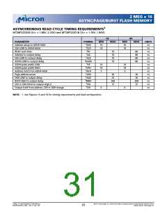
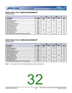
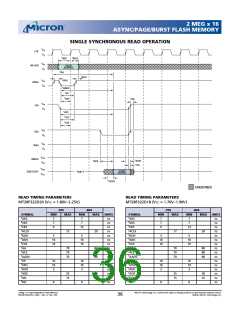
BURST READ CYCLE TIMING REQUIREMENTS
(MT28F322D20)
-705
-804
PARAMETER
CLK period
SYMBOL
MIN
18.5
5
MAX
MIN
25
7.5
MAX
UNITS
ns
ns
ns
ns
ns
ns
ns
ns
t
CLK
t
CLK HIGH (LOW) time
CLK fall (rise) time
Address valid setup to CLK
ADV# LOW setup to CLK
CE# LOW setup to CLK
CLK to output delay
Output hold from CLK
Address hold from CLK
CLK to WAIT# delay
KP
t
KHKL
AKS
3
5
t
7
7
9
7
7
13
t
VKS
CKS
t
t
ACLK
KOH
AKH
KHTL
15
15
20
20
t
3.5
10
5
10
t
ns
ns
ns
t
t
CE# HIGH between subsequent synchronous READs
CBPH
20
20
1
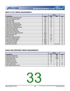
BURST READ CYCLE TIMING REQUIREMENTS
(MT28F322D18)
-705
-804
PARAMETER
CLK period
SYMBOL
MIN
19.2
5
MAX
MIN
25
7.5
MAX
UNITS
ns
ns
ns
ns
ns
ns
ns
ns
t
CLK
t
CLK HIGH (LOW) time
CLK fall (rise) time
Address valid setup to CLK
ADV# LOW setup to CLK
CE# LOW setup to CLK
CLK to output delay
Output hold from CLK
Address hold from CLK
CLK to WAIT# delay
KP
t
KHKL
AKS
3
5
t
7
7
9
7
7
13
t
VKS
CKS
t
t
ACLK
17
15
20
20
t
KOH
AKH
KHTL
3.5
10
5
10
t
ns
ns
ns
t
t
CE# HIGH between subsequent synchronous READs
CBPH
20
20
NOTE: 1. See Figures 15 and 16 for timing requirements and load configuration.
2 Meg x 16 Async/Page/Burst Flash Memory
MT28F322D20FH_4.p65 – Rev. 4, Pub. 7/02
Micron Technology, Inc., reserves the right to change products or specifications without notice.
©2002, Micron Technology, Inc.
32

 MICRON [ MICRON TECHNOLOGY ]