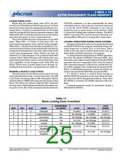
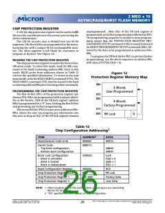
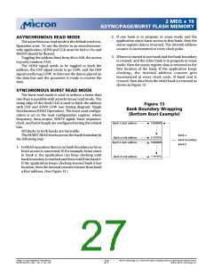
2 MEG x 16
ASYNC/PAGE/BURST FLASH MEMORY
*Stresses greater than those listed under “Absolute Maxi-
mum Ratings” may cause permanent damage to the de-
vice. This is a stress rating only and functional operation
of the device at these or any other conditions above those
indicated in the operational sections of this specification
is not implied. Exposure to absolute maximum rating
conditions for extended periods may affect reliability.
**Maximum DC voltage on VPP may overshoot to +13.5V
for periods < 20ns.
ABSOLUTE MAXIMUM RATINGS*
Voltage to Any Ball Except VCC and VPP
with Respect to VSS ........................ -0.5V to +2.45V
VPP Voltage (for BLOCK ERASE and PROGRAM
with Respect to VSS) .................... -0.5V to +13.5V**
VCC and VCCQ Supply Voltage
with Respect to VSS ........................ -0.3V to +2.45V
Output Short Circuit Current ................................ 100mA
Operating Temperature Range ................ -40oC to +85oC
Storage Temperature Range .................. -55oC to +125oC
Soldering Cycle ............................................. 260oC for 10s
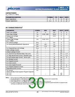
RECOMMENDED OPERATING CONDITIONS
PARAMETER
SYMBOL
MIN
-40
1.80
1.70
1.80
1.70
0.9
MAX
+85
UNITS
oC
NOTES
Operating temperature
tA
VCC supply voltage (MT28F322D20)
VCC supply voltage (MT28F322D18)
I/O supply voltage (MT28F322D20)
I/O supply voltage (MT28F322D18)
VPP voltage
VCC
2.20
V
VCC
1.90
V
VCCQ
VCCQ
VPP1
VPP2
2.25
V
V
1.90
2.25
V
VPP in-factory programming voltage
Block erase cycling (VPP = VPP1)
Block erase cycling (VPP = VPP2)
11.4
–
12.6
V
100,000
100
Cycles
Cycles
–
1
NOTE: 1. VPP = VPP2 is a maximum of 10 cumulative hours.
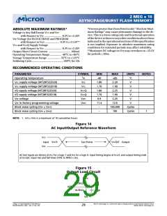
Figure 14
AC Input/Output Reference Waveform
VCC
V
CC/2
VCCQ/2
Input
Test Points
Output
VSS
AC test inputs are driven at VCC for a logic 1 and VSS for a logic 0. Input timing begins at VCC/2, and output timing ends
at VCCQ/2. Input rise and fall times (10% to 90%) < 5ns.
Figure 15
Output Load Circuit
VCC
14.5K
14.5K
I/O
30pF
VSS
2 Meg x 16 Async/Page/Burst Flash Memory
MT28F322D20FH_4.p65 – Rev. 4, Pub. 7/02
Micron Technology, Inc., reserves the right to change products or specifications without notice.
©2002, Micron Technology, Inc.
29

 MICRON [ MICRON TECHNOLOGY ]