2 MEG x 16
ASYNC/PAGE/BURST FLASH MEMORY
ASYNCHRONOUS PAGE READ MODE
After power-up or reset, the device operates in page
mode over the whole memory array. The page size can be
customized at the factory to four or eight words as re-
quired; but if no specification is made, the normal size is
eight words. The initial portion of the page mode cycle is
the same as the asynchronous access cycle. ꢁolding CE#
LOW and toggling addresses A0–A2 allows random ac-
cess of other words in the page.
STANDBY MODE
ICC supplycurrentisreducedbyapplyingalogicꢁIGꢁ
level on CE# and RST# to enter the standby mode. In the
standby mode, the outputs are ꢁigh-Z. Applying a CMOS
logic ꢁIGꢁ level on CE# and RST# reduces the current to
ICC4 (MAX). If the device is deselected during an ERASE
operation or during programming, the device continues
to draw current until the operation is complete.
AUTOMATIC POWER SAVE MODE (APS)
Substantial power savings are realized during periods
when the array is not being read and the device is in the
active mode. During this time the device switches to the
automatic power save mode. When the device switches
to this mode, ICC is reduced to a level comparable to ICC4.
Further power savings can be realized by applying a logic
ꢁIGꢁ level to CE# to place the device in standby mode.
The low level of power is maintained until another opera-
tion is initiated. In this mode, the I/Os retain the data
from the last memory address read until a new address is
read. This mode is entered automatically if no address or
control signals toggle.
VPP/VCC PROGRAM AND ERASE
VOLTAGES
The Flash devices provide in-system programming
and erase with VPP in the 0.9V–2.2V range (VPP1). The 12V
VPP (VPP2) mode programming is offered for compatibil-
ity with existing programming equipment.
The device can withstand 100,000 WRITE/ERASE op-
erationswhenVPP =VPP1 or100WRITE/ERASEoperations
and 10 cumulative hours when VPP = VPP2.
In addition to the flexible block locking, the VPP
programmingvoltagecanbeheldLOWforabsolutehard-
ware write protection of all blocks in the Flash device.
When VPP is below VPPLK, any PROGRAM or ERASE opera-
tion will result in an error, prompting the corresponding
status register bit (SR3) to be set.
DuringWRITEandERASEoperations,theWSMmoni-
tors the VPP voltage level. WRITE/ERASE operations are
allowed only when VPP is within the ranges specified in
Table 13.
When VCC is below VLKO or VPP is below VPPLK, any
WRITE/ERASE operation will be prevented.
DEVICE RESET
To correctly reset the Flash devices, the RST# signal
must be asserted (RST# = VIL) for a minimum of tRP. After
reset, the devices can be accessed for a READ operation
with a delayed access time of tRWꢁ from the rising edge
ofRST#. ThecircuitryusedforgeneratingtheRST#signal
needs to be common with the rest of the system reset to
ensure that correct system initialization occurs. Please
refer to the timing diagram for further details.
POWER-UP SEQUENCE
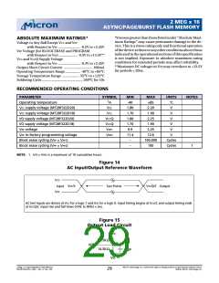
Table 13
VPP Range (V)
The following power-up sequence is recommended
to properly initialize internal chip operations:
• Atpower-up, RST#shouldbekeptatVIL for2µsafter
VCC reaches VCC (MIN).
MIN
0.9
MAX
2.25
12.6
• VCCQ should not come up before VCC.
In System (VPP1)
In Factory (VPP2)
• VPP should be kept atVIL to maximize data integrity.
When the power-up sequence is completed, RST#
should be brought to VIꢁ. To ensure a proper power-up,
the rise time of RST (10ꢀ–90ꢀ) should be < 10µs.
11.4
2 Meg x 16 Async/Page/Burst Flash Memory
MT28F322D20FH_4.p65 – Rev. 4, Pub. 7/02
Micron Technology, Inc., reserves the right to change products or specifications without notice.
28
©2002, Micron Technology, Inc.

 MICRON [ MICRON TECHNOLOGY ]