2 MEG x 16
ASYNC/PAGE/BURST FLASH MEMORY
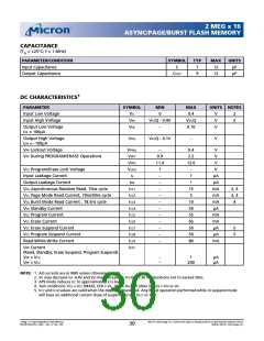
CHIP PROTECTION REGISTER
unprogrammed. After DQ1 of the PR lock register is
programmed, nofurtherprogrammingisallowedonPR2.
The programming sequence is similar to array program-
ming except that the PROTECTION REGISTER PRO-
GRAMMING SETUP command (C0h) is issued instead of
an ARRAY PROGRAMMING SETUP command (40h), fol-
lowed by the data to be programmed at addresses 85h–
88h.
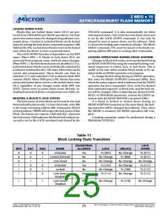
A 128-bit chip protection register can be used to fulfill
the security considerations in the system (preventing the
device substitution).
The 128-bit security area is divided into two 64-bit
segments. The first 64 bits are programmed at the manu-
facturing site with a unique 64-bit unchangeable num-
ber. The other segment is left blank for customers to
program as desired. (See Figure 12).
To program the PR lock bit for PR2 (to prevent further
programming), use the above sequence on address 80h,
with data of FFFDh (DQ1 = 0).
READING THE CHIP PROTECTION REGISTER
The chip protection register is read in the device iden-
tification mode. To enter this mode, load the 90h com-
mand to the bank containing address 00h. Once in this
mode, READ cycles from addresses shown in Table 12
retrieve the specified information. To return to the read
array mode, write the READ ARRAY command (FFh). The
READ ARRAY command, FFh, must be issued to the bank
containingaddress00hpriortoissuingothercommands.
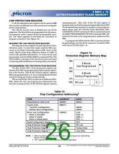
Figure 12
Protection Register Memory Map
88h
4 Words
User-Programmed
PROGRAMMING THE CHIP PROTECTION REGISTER
The first 64 bits (PR1) of the protection register (ad-
dresses 81h–84h) are programmed with a unique identi-
fier at the factory. DQ0 of the PR lock register (address
80h) is programmed to a “0” state, locking the first 64 bits
and preventing any further programming.
The second 64 bits (PR2) is a user area (addresses 85h–
88h), where the user can program any information into
this area as long as DQ1 of the PR lock register remains
85h
84h
4 Words
Factory-Programmed
81h
80h
PR Lock
0
Table 12
Chip Configuration Addressing
1
ITEM
ADDRESS2
00000h
DATA
Manufacturer Code (x16)
002Ch
Device Code
00001h
Top boot configuration
Bottom boot configuration
44B4h
44B5h
·
·
Block Lock Configuration
XX002h
Lock
Block is unlocked
Block is locked
Block is locked down
DQ0 = 0
DQ0 = 1
DQ1 = 1
·
·
·
Read Configuration Register
Chip Protection Register Lock
Chip Protection Register 1
Chip Protection Register 2
00005h
80h
RCR
PR Lock
81h–84h
85h–88h
Factory Data
User Data
NOTE: 1. Other locations within the configuration address space are reserved by
Micron for future use.
2. “XX” specifies the block address of lock configuration.
2 Meg x 16 Async/Page/Burst Flash Memory
MT28F322D20FH_4.p65 – Rev. 4, Pub. 7/02
Micron Technology, Inc., reserves the right to change products or specifications without notice.
©2002, Micron Technology, Inc.
26

 MICRON [ MICRON TECHNOLOGY ]