2 MEG x 16
ASYNC/PAGE/BURST FLASH MEMORY
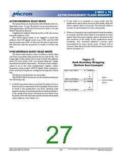
2. If one bank is in program or erase mode and the
application starts burst access in that bank, then the
status register data is returned. The internal address
counter is incremented at every clock pulse.
ASYNCHRONOUS READ MODE
The asynchronous read mode is the default read con-
figuration state. To use the device in an asynchronous-
only application, ADV# and CLK must be tied to VSS and
WAIT# should be floated.
3. If burst is started in one bank and the bank boundary
is crossed, and the other bank is in program or erase
mode, then the status register data is returned as the
first location of the bank. If the application keeps
clocking, the internal address counter gets
incremented at every clock cycle. If bank end is
crossed, then data from the other bank is returned as
shown in Figure 13.
Toggling the address lines from A0 to A20, the access
is purely random (tAA).
The ADV# signal needs to be toggled to latch the
address, the CE# signal needs to go LOW, and the OE#
signal needs to go LOW. In this case the data is placed on
the data bus and the processor is ready to receive the
data.
SYNCHRONOUS BURST READ MODE
The burst read mode is used to achieve a faster data
rate than is possible with asynchronous read mode. The
rising edge of the clock CLK is used to latch the address
with CE# and ADV# LOW (see timing diagram: Single
Synchronous READ Operation). The burst read configu-
ration is set in the read configuration register, where
frequency, data output, WAIT# signal, burst sequence,
clock, and burst length are configured setting the related
bits.
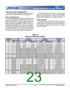
Figure 13
Bank Boundary Wrapping
(Bottom Boot Example)
Bank a start address
0 00000h
All blocks in both banks are burstable.
The BURST READ works across the bank boundary in
the following way:
Bank a
Bank a end address
Bank b start address
0 7FFFFh
0 80000h
bank boundary
Bank b
1. In READ operation there is no bank boundary as far as
burst access is concerned. If, for example, burst starts
in bank a, the application can keep clocking until
bank boundary is reached and then read from bank b.
If the application keeps clocking beyond bank b last
location, then the internal counter restarts from bank
a first address. (See Figure 13.)
Bank b end address
1 FFFFFh
2 Meg x 16 Async/Page/Burst Flash Memory
MT28F322D20FH_4.p65 – Rev. 4, Pub. 7/02
Micron Technology, Inc., reserves the right to change products or specifications without notice.
©2002, Micron Technology, Inc.
27

 MICRON [ MICRON TECHNOLOGY ]