2 MEG x 16
ASYNC/PAGE/BURST FLASH MEMORY
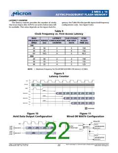
HOLD DATA OUTPUT CONFIGURATION
The hold data output configuration specifies for how
many clocks data will be held valid. (See Figure 10.)
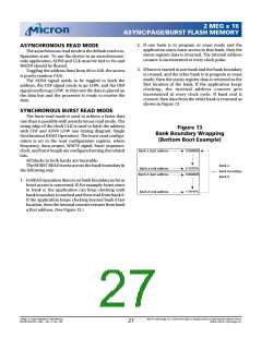
A Flash controller (CPU) is able to use this output
signal to drive banks of the devices. An internal 1MΩ
pull-up resistor holds WAIT# = 1 and allows wired OR’ing
multiple bank configurations, as shown in Figure 11.
WAIT# CONFIGURATION
The wait configuration bit, RCR8, sets the behavior of
the WAIT# output signal. The WAIT# signal can be active
during an output delay or one data cycle before delay
when continuous burst length is enabled. WAIT# = 1
indicates valid data when RCR8 = 0. WAIT# = 0 indicates
invalid data when RCR8 = 0. The setting of wait before or
wait during RCR8 will depend on the system and CPU
characteristic. If RCR3 = 1 (no wrap mode), then WAIT#
can also be enabled in a four- or eight-word burst if the
no-wrap burst crosses the first eight-word boundary.
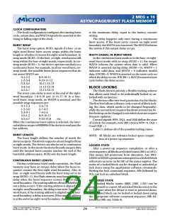
BURST SEQUENCE
The burst sequence specifies the address order of the
data in synchronous burst mode. It can be programmed
as either linear or interleaved burst order. Continuous
burst length only supports linear burst order. See Table
10 for more details.
Table 10
Sequence and Burst Length
STARTING
NO
4-WORD
BURST LENGTH
8-WORD
BURST LENGTH
CONTINUOUS
BURST
ADDRESS
WRAP WRAP
.
(DEC)
0
RCR3
RCR3
LINEAR
INTERLEAVED
0-1-2-3
LINEAR
INTERLEAVED
0-1-2-3-4-5-6-7
1-0-3-2-5-4-7-6
2-3-0-1-6-7-4-5
3-2-1-0-7-6-5-4
4-5-6-7-0-1-2-3
5-4-7-6-1-0-3-2
6-7-4-5-2-3-0-1
7-6-5-4-3-2-1-0
...
LINEAR
0-1-2-3-4-5-6-…
1-2-3-4-5-6-7-…
2-3-4-5-6-7-8-…
3-4-5-6-7-8-9-…
4-5-6-7-8-9-10-…
5-6-7-8-9-10-11-…
6-7-8-9-10-11-12-…
6-7-8-9-10-11-12-13-…
...
0
0
0
0
0
0
0
0
...
0
0
...
0-1-2-3
1-2-3-0
2-3-0-1
3-0-1-2
0-1-2-3-4-5-6-7
1-2-3-4-5-6-7-0
2-3-4-5-6-7-0-1
3-4-5-6-7-0-1-2
4-5-6-7-0-1-2-3
5-6-7-0-1-2-3-4
6-7-0-1-2-3-4-5
7-0-1-2-3-4-5-6
...
1
1-0-3-2
2
3
4
5
6
7
...
14
15
...
0
1
2
3
4
2-3-0-1
3-2-1-0
...
...
...
14-15-16-17-18-19-20-..
15-16-17-18-19-20-21-..
...
...
1
1
1
1
1
1
1
1
...
1
1
...
...
...
...
0-1-2-3
1-2-3-4
2-3-4-5
3-4-5-6
NA
NA
NA
NA
0-1-2-3-4-5-6-7
1-2-3-4-5-6-7-8
2-3-4-5-6-7-8-9
3-4-5-6-7-8-9-10
4-5-6-7-8-9-10-11
5-6-7-8-9-10-11-12
6-7-8-9-10-11-12-13
7-8-9-10-11-12-13-14
...
NA
NA
NA
NA
NA
NA
NA
NA
...
0-1-2-3-4-5-6-…
1-2-3-4-5-6-7-…
2-3-4-5-6-7-8-…
3-4-5-6-7-8-9-…
4-5-6-7-8-9-10-…
5-6-7-8-9-10-11…
6-7-8-9-10-11-12…
7-8-9-10-11-12-13…
...
5
6
7
...
14
15
…
...
...
...
...
14-15-16-17-18-19-20-…
15-16-17-18-19-20-21-…
2 Meg x 16 Async/Page/Burst Flash Memory
MT28F322D20FH_4.p65 – Rev. 4, Pub. 7/02
Micron Technology, Inc., reserves the right to change products or specifications without notice.
©2002, Micron Technology, Inc.
23

 MICRON [ MICRON TECHNOLOGY ]