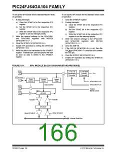
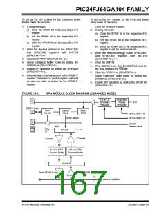
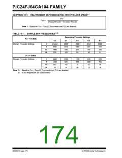
PIC24FJ64GA104 FAMILY
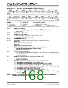
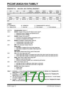
REGISTER 15-2: SPIXCON1: SPIx CONTROL REGISTER 1
U-0
—
U-0
—
U-0
—
R/W-0
DISSCK(1)
R/W-0
DISSDO(2)
R/W-0
R/W-0
SMP
R/W-0
CKE(3)
MODE16
bit 15
bit 8
R/W-0
SSEN(4)
R/W-0
CKP
R/W-0
R/W-0
R/W-0
R/W-0
R/W-0
R/W-0
MSTEN
SPRE2
SPRE1
SPRE0
PPRE1
PPRE0
bit 7
bit 0
Legend:
R = Readable bit
-n = Value at POR
W = Writable bit
‘1’ = Bit is set
U = Unimplemented bit, read as ‘0’
‘0’ = Bit is cleared x = Bit is unknown
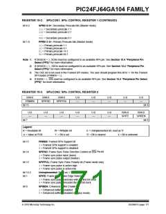
bit 15-13
bit 12
Unimplemented: Read as ‘0’
DISSCK: Disable SCKx pin bit (SPI Master modes only)(1)
1= Internal SPI clock is disabled; pin functions as I/O
0= Internal SPI clock is enabled
bit 11
bit 10
bit 9
DISSDO: Disable SDOx pin bit(2)
1= SDOx pin is not used by module; pin functions as I/O
0= SDOx pin is controlled by the module
MODE16: Word/Byte Communication Select bit
1= Communication is word-wide (16 bits)
0= Communication is byte-wide (8 bits)
SMP: SPIx Data Input Sample Phase bit
Master mode:
1= Input data is sampled at the end of data output time
0= Input data is sampled at the middle of data output time
Slave mode:
SMP must be cleared when SPIx is used in Slave mode.
bit 8
bit 7
bit 6
bit 5
CKE: SPIx Clock Edge Select bit(3)
1= Serial output data changes on transition from active clock state to Idle clock state (see bit 6)
0= Serial output data changes on transition from Idle clock state to active clock state (see bit 6)
SSEN: Slave Select Enable (Slave mode) bit(4)
1= SSx pin is used for Slave mode
0= SSx pin is not used by module; pin is controlled by port function
CKP: Clock Polarity Select bit
1= Idle state for clock is a high level; active state is a low level
0= Idle state for clock is a low level; active state is a high level
MSTEN: Master Mode Enable bit
1= Master mode
0= Slave mode
Note 1: If DISSCK = 0, SCKx must be configured to an available RPn pin. See Section 10.4 “Peripheral Pin
Select (PPS)” for more information.
2: If DISSDO = 0, SDOx must be configured to an available RPn pin. See Section 10.4 “Peripheral Pin
Select (PPS)” for more information.
3: The CKE bit is not used in the Framed SPI modes. The user should program this bit to ‘0’ for the Framed
SPI modes (FRMEN = 1).
4: If SSEN = 1, SSx must be configured to an available RPn pin. See Section 10.4 “Peripheral Pin Select
(PPS)” for more information.
DS39951C-page 170
2010 Microchip Technology Inc.

 MICROCHIP [ MICROCHIP ]