PIC24FJ64GA104 FAMILY
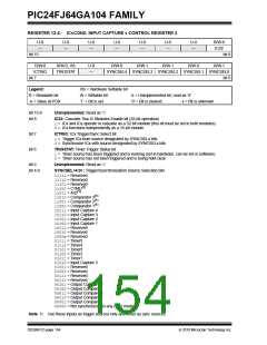
REGISTER 13-2: ICxCON2: INPUT CAPTURE x CONTROL REGISTER 2
U-0
—
U-0
—
U-0
—
U-0
—
U-0
—
U-0
—
U-0
—
R/W-0
IC32
bit 15
bit 8
R/W-0
R/W-0, HS
TRIGSTAT
U-0
—
R/W-0
R/W-1
R/W-1
R/W-0
R/W-1
ICTRIG
SYNCSEL4 SYNCSEL3 SYNCSEL2 SYNCSEL1 SYNCSEL0
bit 0
bit 7
Legend:
HS = Hardware Settable bit
W = Writable bit
R = Readable bit
-n = Value at POR
U = Unimplemented bit, read as ‘0’
‘0’ = Bit is cleared x = Bit is unknown
‘1’ = Bit is set
bit 15-9
bit 8
Unimplemented: Read as ‘0’
IC32: Cascade Two IC Modules Enable bit (32-bit operation)
1= ICx and ICy operate in cascade as a 32-bit module (this bit must be set in both modules)
0= ICx functions independently as a 16-bit module
bit 7
bit 6
ICTRIG: ICx Trigger/Sync Select bit
1= Trigger ICx from source designated by SYNCSELx bits
0= Synchronize ICx with source designated by SYNCSELx bits
TRIGSTAT: Timer Trigger Status bit
1= Timer source has been triggered and is running (set in hardware, can be set in software)
0= Timer source has not been triggered and is being held clear
bit 5
Unimplemented: Read as ‘0’
bit 4-0
SYNCSEL<4:0>: Trigger/Synchronization Source Selection bits
11111= Reserved
11110= Reserved
11101= Reserved
11100= CTMU(1)
11011= A/D(1)
11010= Comparator 3(1)
11001= Comparator 2(1)
11000= Comparator 1(1)
10111= Input Capture 4
10110= Input Capture 3
10101= Input Capture 2
10100= Input Capture 1
10011= Reserved
10010= Reserved
1000x= Reserved
01111= Timer5
01110= Timer4
01101= Timer3
01100= Timer2
01011= Timer1
01010= Input Capture 5
01001= Reserved
01000= Reserved
00111= Reserved
00110= Reserved
00101= Output Compare 5
00100= Output Compare 4
00011= Output Compare 3
00010= Output Compare 2
00001= Output Compare 1
00000= Not synchronized to any other module
Note 1: Use these inputs as trigger sources only and never as sync sources.
DS39951C-page 154
2010 Microchip Technology Inc.

 MICROCHIP [ MICROCHIP ]