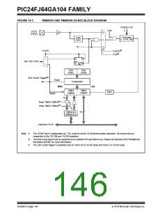
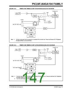
PIC24FJ64GA104 FAMILY
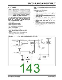
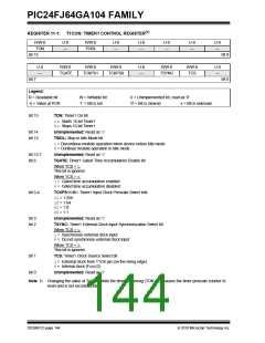
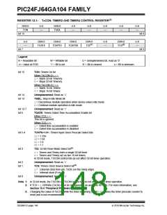
REGISTER 11-1: T1CON: TIMER1 CONTROL REGISTER(1)
R/W-0
TON
U-0
—
R/W-0
TSIDL
U-0
—
U-0
—
U-0
—
U-0
—
U-0
—
bit 15
bit 8
bit 0
U-0
—
R/W-0
R/W-0
R/W-0
U-0
—
R/W-0
R/W-0
TCS
U-0
—
TGATE
TCKPS1
TCKPS0
TSYNC
bit 7
Legend:
R = Readable bit
-n = Value at POR
W = Writable bit
‘1’ = Bit is set
U = Unimplemented bit, read as ‘0’
‘0’ = Bit is cleared x = Bit is unknown
bit 15
TON: Timer1 On bit
1= Starts 16-bit Timer1
0= Stops 16-bit Timer1
bit 14
bit 13
Unimplemented: Read as ‘0’
TSIDL: Stop in Idle Mode bit
1= Discontinue module operation when device enters Idle mode
0= Continue module operation in Idle mode
bit 12-7
bit 6
Unimplemented: Read as ‘0’
TGATE: Timer1 Gated Time Accumulation Enable bit
When TCS = 1:
This bit is ignored.
When TCS = 0:
1= Gated time accumulation enabled
0= Gated time accumulation disabled
bit 5-4
TCKPS<1:0>: Timer1 Input Clock Prescale Select bits
11= 1:256
10= 1:64
01= 1:8
00= 1:1
bit 3
bit 2
Unimplemented: Read as ‘0’
TSYNC: Timer1 External Clock Input Synchronization Select bit
When TCS = 1:
1= Synchronize external clock input
0= Do not synchronize external clock input
When TCS = 0:
This bit is ignored.
bit 1
bit 0
TCS: Timer1 Clock Source Select bit
1= External clock from T1CK pin (on the rising edge)
0= Internal clock (FOSC/2)
Unimplemented: Read as ‘0’
Note 1: Changing the value of TxCON while the timer is running (TON = 1) causes the timer prescale counter to
reset and is not recommended.
DS39951C-page 144
2010 Microchip Technology Inc.

 MICROCHIP [ MICROCHIP ]