PIC24FJ64GA104 FAMILY
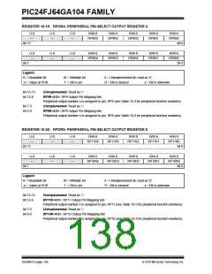
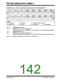
REGISTER 10-27: RPOR12: PERIPHERAL PIN SELECT OUTPUT REGISTER 12(1)
U-0
—
U-0
—
U-0
—
R/W-0
R/W-0
R/W-0
R/W-0
R/W-0
RP25R4
RP25R3
RP25R2
RP25R1
RP25R0
bit 15
bit 8
U-0
—
U-0
—
U-0
—
R/W-0
R/W-0
R/W-0
R/W-0
R/W-0
RP24R4
RP24R3
RP24R2
RP24R1
RP24R0
bit 7
bit 0
Legend:
R = Readable bit
-n = Value at POR
W = Writable bit
‘1’ = Bit is set
U = Unimplemented bit, read as ‘0’
‘0’ = Bit is cleared x = Bit is unknown
bit 15-13
bit 12-8
Unimplemented: Read as ‘0’
RP25R<5:0>: RP25 Output Pin Mapping bits
Peripheral output number n is assigned to pin, RP25 (see Table 10-3 for peripheral function numbers).
Unimplemented: Read as ‘0’
bit 7-5
bit 4-0
RP24R<5:0>: RP24 Output Pin Mapping bits
Peripheral output number n is assigned to pin, RP24 (see Table 10-3 for peripheral function numbers).
Note 1: This register is unimplemented in 28-pin devices; all bits read as ‘0’.
DS39951C-page 142
2010 Microchip Technology Inc.

 MICROCHIP [ MICROCHIP ]