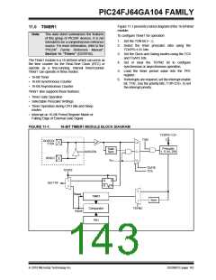
PIC24FJ64GA104 FAMILY
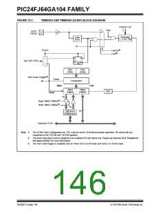
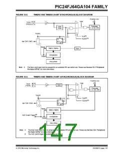
FIGURE 12-2:
TIMER2 AND TIMER4 (16-BIT SYNCHRONOUS) BLOCK DIAGRAM
TCKPS<1:0>
2
TON
T2CK
(T4CK)
1x
Prescaler
1, 8, 64, 256
Gate
Sync
01
00
TGATE
(1)
TCS
TGATE
TCY
(1)
Q
D
1
0
Set T2IF (T4IF)
Q
CK
Reset
Equal
TMR2 (TMR4)
Sync
Comparator
PR2 (PR4)
Note 1: The timer clock input must be assigned to an available RPn pin before use. Please see Section 10.4 “Peripheral
Pin Select (PPS)” for more information.
FIGURE 12-3:
TIMER3 AND TIMER5 (16-BIT ASYNCHRONOUS) BLOCK DIAGRAM
TCKPS<1:0>
2
TON
T3CK
(T5CK)
1x
01
00
Sync
Prescaler
1, 8, 64, 256
TGATE
(1)
TCS
TGATE
TCY
(1)
Q
Q
D
1
0
Set T3IF (T5IF)
CK
Reset
Equal
TMR3 (TMR5)
(2)
ADC Event Trigger
Comparator
PR3 (PR5)
Note 1: The timer clock input must be assigned to an available RPn pin before use. Please see Section 10.4 “Peripheral
Pin Select (PPS)” for more information.
2: The ADC event trigger is available only on Timer3.
2010 Microchip Technology Inc.
DS39951C-page 147

 MICROCHIP [ MICROCHIP ]