PIC24FJ64GA104 FAMILY
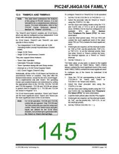
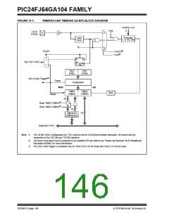
FIGURE 12-1:
TIMER2/3 AND TIMER4/5 (32-BIT) BLOCK DIAGRAM
TCKPS<1:0>
2
TON
T2CK
(T4CK)
1x
Prescaler
1, 8, 64, 256
Gate
01
00
Sync
TCY
(2)
TGATE
TGATE
(2)
TCS
1
0
Q
D
Set T3IF (T5IF)
Q
CK
PR3
PR2
(PR5)
(PR4)
(3)
ADC Event Trigger
Equal
MSB
Comparator
LSB
TMR2
(TMR4)
TMR3
(TMR5)
Sync
Reset
16
(1)
(1)
Read TMR2 (TMR4)
Write TMR2 (TMR4)
16
16
TMR3HLD
(TMR5HLD)
Data Bus<15:0>
Note 1: The 32-Bit Timer Configuration bit, T32, must be set for 32-bit timer/counter operation. All control bits are
respective to the T2CON and T4CON registers.
2: The timer clock input must be assigned to an available RPn pin before use. Please see Section 10.4 “Peripheral
Pin Select (PPS)” for more information.
3: The ADC event trigger is available only on Timer 2/3 in 32-bit mode and Timer 3 in 16-bit mode.
DS39951C-page 146
2010 Microchip Technology Inc.

 MICROCHIP [ MICROCHIP ]