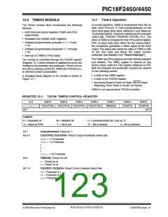
PIC18F2450/4450
13.3.3
SOFTWARE INTERRUPT MODE
13.3 Compare Mode
When the Generate Software Interrupt mode is chosen
(CCP1M3:CCP1M0 = 1010), the CCP1 pin is not
affected. Only a CCP interrupt is generated, if enabled,
and the CCP1IE bit is set.
In Compare mode, the 16-bit CCPR1 register value is
constantly compared against the TMR1 register pair
value. When a match occurs, the CCP1 pin can be:
• driven high
• driven low
13.3.4
SPECIAL EVENT TRIGGER
• toggled (high-to-low or low-to-high)
The CCP module is equipped with a Special Event
Trigger. This is an internal hardware signal generated
in Compare mode to trigger actions by other modules.
The Special Event Trigger is enabled by selecting
the Compare Special Event Trigger mode
(CCP1M3:CCP1M0 = 1011).
• remain unchanged (that is, reflects the state of the
I/O latch)
The action on the pin is based on the value of the mode
select bits (CCP1M3:CCP1M0). At the same time, the
interrupt flag bit, CCP1IF, is set.
For the CCP module, the Special Event Trigger resets
the Timer1 register pair. This allows the CCPR1
registers to serve as a programmable period register
for the Timer1.
13.3.1
CCP1 PIN CONFIGURATION
The user must configure the CCP1 pin as an output by
clearing the appropriate TRIS bit.
The Special Event Trigger for CCP1 can also start an
A/D conversion. In order to do this, the A/D converter
must already be enabled.
Note:
Clearing the CCP1CON register will force
the RC2 compare output latch to the
default low level.
13.3.2
TIMER1 MODE SELECTION
Timer1 must be running in Timer mode, or
Synchronized Counter mode, if the CCP module is
using the compare feature. In Asynchronous Counter
mode, the compare operation may not work.
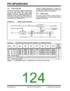
FIGURE 13-2:
COMPARE MODE OPERATION BLOCK DIAGRAM
Special Event Trigger
(Timer1 Reset)
Set CCP1IF
CCPR1H
CCPR1L
CCP1 pin
S
R
Q
Output
Logic
Compare
Match
Comparator
TRIS
Output Enable
4
CCP1CON<3:0>
TMR1H
TMR1L
© 2006 Microchip Technology Inc.
Advance Information
DS39760A-page 125

 MICROCHIP [ MICROCHIP ]