PIC18F2450/4450
A range of 16 postscale options (from 1:1 through 1:16
inclusive) can be selected with the postscaler control
bits, T2OUTPS3:T2OUTPS0 (T2CON<6:3>).
12.2 Timer2 Interrupt
Timer2 also can generate an optional device interrupt.
The Timer2 output signal (TMR2 to PR2 match)
provides the input for the 4-bit output counter/
postscaler. This counter generates the TMR2 match
interrupt flag which is latched in TMR2IF (PIR1<1>).
The interrupt is enabled by setting the TMR2 Match
Interrupt Enable bit, TMR2IE (PIE1<1>).
12.3 TMR2 Output
The unscaled output of TMR2 is available primarily to
the CCP module, where it is used as a time base for
operations in PWM mode.
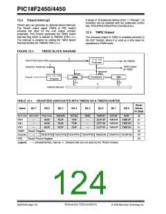
FIGURE 12-1:
TIMER2 BLOCK DIAGRAM
4
1:1 to 1:16
Set TMR2IF
Postscaler
T2OUTPS3:T2OUTPS0
2
TMR2 Output
T2CKPS1:T2CKPS0
(to PWM)
TMR2/PR2
Match
Reset
TMR2
1:1, 1:4, 1:16
Prescaler
Comparator
PR2
FOSC/4
8
8
8
Internal Data Bus
TABLE 12-1: REGISTERS ASSOCIATED WITH TIMER2 AS A TIMER/COUNTER
Reset
Values
on page
Name
Bit 7
Bit 6
Bit 5
Bit 4
Bit 3
Bit 2
Bit 1
Bit 0
INTCON GIE/GIEH PEIE/GIEL TMR0IE
INT0IE
TXIF
RBIE
—
TMR0IF
CCP1IF
CCP1IE
CCP1IP
INT0IF
TMR2IF
TMR2IE
TMR2IP
RBIF
49
51
51
51
50
50
50
PIR1
PIE1
IPR1
—
—
—
ADIF
ADIE
ADIP
RCIF
RCIE
RCIP
TMR1IF
TMR1IE
TMR1IP
TXIE
TXIP
—
—
TMR2 Timer2 Register
T2CON
PR2
—
T2OUTPS3 T2OUTPS2 T2OUTPS1 T2OUTPS0 TMR2ON T2CKPS1 T2CKPS0
Timer2 Period Register
Legend: — = unimplemented, read as ‘0’. Shaded cells are not used by the Timer2 module.
DS39760A-page 122
Advance Information
© 2006 Microchip Technology Inc.

 MICROCHIP [ MICROCHIP ]